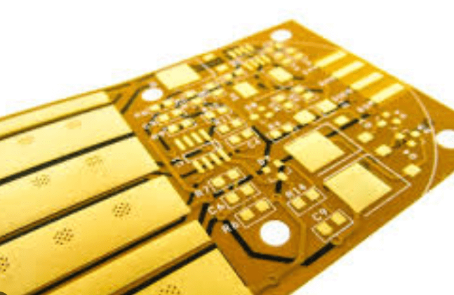
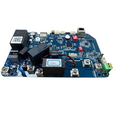
High speed pcb design guidelines
1. High-Speed Digital Design: A Handbook of Black Magic by Howard Johnson and Martin Graham
2. Signal and Power Integrity – Simplified by Eric Bogatin
3. Principles of Signal Integrity by Dr. Howard Johnson
4. PCB Design for High-Speed Digital Systems by Dr. Lee Ritchey
5. High-Speed PCB Design Considerations by Altium
6. High-Speed Board Design Techniques by Cadence
7. High-Speed PCB Layout Guidelines by Texas Instruments
8. High-Speed PCB Design and Analysis by ANSYS
9. High-Speed Design Techniques by Mentor Graphics
10. High-Speed PCB Design Best Practices by Sierra Circuits.

Here are some high-speed PCB design guidelines:
1. Keep signal traces as short as possible to minimize signal delay and reduce noise.
2. Use high-quality materials for the PCB substrate and copper layers to minimize signal loss and improve signal integrity.
3. Maintain consistent trace widths and spacing to minimize impedance variations.
4. Use differential signaling for high-speed signals to improve noise immunity and reduce crosstalk.
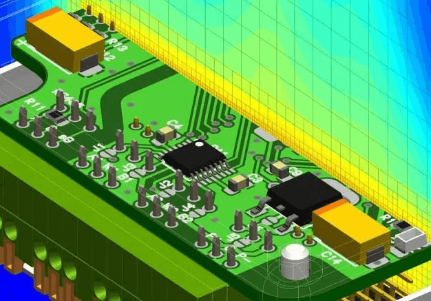
5. Place decoupling capacitors close to the power and ground pins of each IC to provide a low impedance path for high-frequency noise.
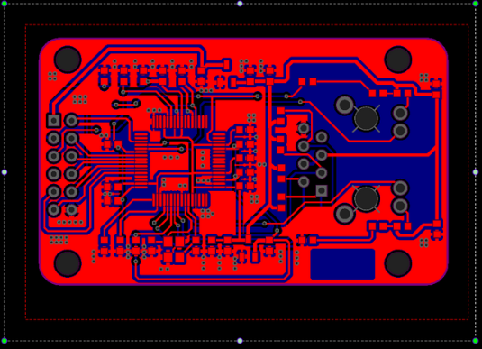
6. Use a ground plane to provide a low impedance return path for signals and to reduce electromagnetic interference (EMI).
7. Minimize the number of vias on signal traces to reduce signal reflection and impedance variations.
8. Use controlled impedance routing for high-speed signals to maintain a consistent impedance throughout the signal path.
9. Use proper termination techniques for high-speed signals, such as series termination or parallel termination.
10. Use EMI shielding techniques, such as shielding cans or grounded shields, to reduce EMI emissions and improve signal integrity.

high speed pcb design guidelines content
1. Introduction to High Speed PCB Design
2. Understanding Signal Integrity
3. PCB Stackup Design
4. Component Placement Considerations
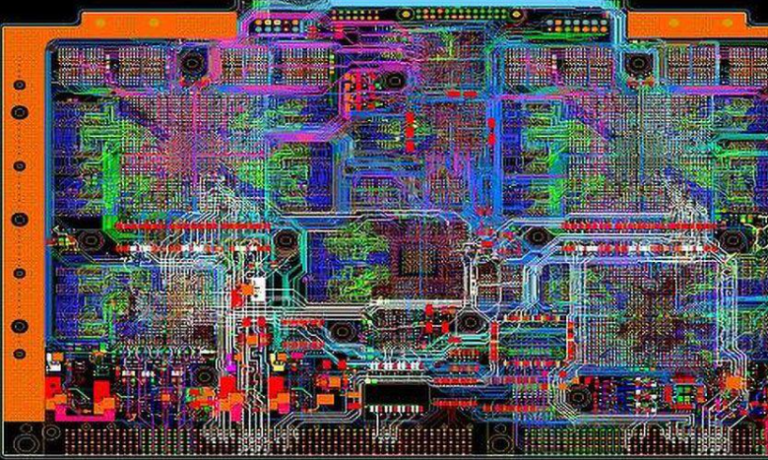
5. Routing Techniques for High Speed Signals
6. Impedance Control and Matching
7. Power and Ground Planes
8. Signal Integrity Analysis and Simulation
9. EMC/EMI Considerations
10. Design for Manufacturability (DFM) and Design for Test (DFT)
11. PCB Material Selection
12. Design Guidelines for High Speed Differential Signals
13. Design Guidelines for High Speed Single-Ended Signals
14. Design Guidelines for High Speed Clock Signals
15. Design Guidelines for High Speed Memory Interfaces
16. Design Guidelines for High Speed Serial Interfaces
17. Design Guidelines for High Speed Power Delivery
18. Design Guidelines for High Speed Signal Integrity Testing
19. Case Studies and Examples of High Speed PCB Designs
20. Conclusion and Future Trends in High Speed PCB Design.
Here are some common high-speed PCB design rules:
1. Keep signal traces as short as possible to reduce signal delay and minimize signal reflections.
2. Maintain a consistent and controlled impedance throughout the signal path to minimize signal reflections and ensure signal integrity.
3. Use a ground plane to provide a low-impedance return path for signals and to reduce electromagnetic interference (EMI).
4. Place decoupling capacitors close to power and ground pins of ICs to reduce noise and voltage fluctuations.
5. Minimize the number of vias and use them only when necessary to reduce signal reflections and impedance discontinuities.
6. Use differential pairs for high-speed signals to reduce noise and crosstalk.
7. Route high-speed signals on inner layers of the PCB to reduce EMI and improve signal integrity.
8. Use a controlled impedance trace width to maintain a consistent impedance throughout the signal path.
9. Avoid sharp corners and right angles in signal traces to reduce signal reflections and EMI.
10. Ensure that the power and ground planes are properly connected through multiple vias to provide a low-impedance return path for signals.
11. Use proper termination techniques for high-speed signals to reduce signal reflections and improve signal integrity.
12. Use simulation and analysis tools to verify signal integrity and EMI performance.
It is important to note that these rules may vary depending on the specific design requirements and the technology used. It is recommended to consult with industry standards and guidelines, as well as experienced PCB designers, to ensure a successful high-speed PCB design.