High-Speed PCB Routing Rules for PCI Express
Introduction
PCI Express (Peripheral Component Interconnect Express), commonly abbreviated as PCIe, has become the standard high-speed serial computer expansion bus architecture since its introduction in 2003. As successive generations have increased data rates from 2.5 GT/s in PCIe 1.0 to 32 GT/s in PCIe 5.0 and beyond, proper PCB layout and routing have become increasingly critical for maintaining signal integrity. This article provides comprehensive guidelines for high-speed PCB routing when designing PCI Express interfaces.
PCI Express Architecture Overview
PCI Express uses a point-to-point architecture with separate transmit and receive differential pairs (lanes). Each lane consists of two differentially routed signals:
- For Gen1/Gen2: 2.5 GT/s and 5 GT/s respectively
- For Gen3: 8 GT/s with 128b/130b encoding
- For Gen4: 16 GT/s
- For Gen5: 32 GT/s
- For Gen6 (emerging): 64 GT/s with PAM4 signaling
The high-speed nature of these signals demands careful attention to impedance control, length matching, crosstalk mitigation, and proper reference plane management.
Fundamental Routing Rules
1. Impedance Control
Maintaining consistent differential impedance is paramount:
- Target impedance: 85Ω differential (±10%) for most implementations
- Single-ended impedance: Typically 50Ω
- Impedance calculation: Affected by trace width, spacing, dielectric thickness, and material properties
Use field solvers or impedance calculators to determine proper geometries for your stackup. Remember that impedance discontinuities at connectors, vias, and package transitions must be minimized.
2. Differential Pair Routing
Proper differential pair routing ensures signal integrity:
- Pair spacing: Maintain consistent spacing between the two traces of a pair (typically 5-8 mil for 85Ω)
- Inter-pair spacing: Keep at least 3× the intra-pair spacing to minimize crosstalk
- Avoid splits: Never route differential pairs over reference plane splits
- Minimize length mismatches: Keep intra-pair length matching within tolerances (discussed below)
3. Length Matching Requirements
Timing skew must be carefully controlled:
- Intra-pair matching:
- Gen1/Gen2: < 5 mil mismatch
- Gen3: < 2 mil mismatch
- Gen4/Gen5: < 1 mil mismatch
- Inter-pair matching (for multiple lanes):
- Gen1/Gen2: < 50 mil between lanes
- Gen3: < 20 mil between lanes
- Gen4/Gen5: < 10 mil between lanes
Use serpentine routing for length matching, but avoid sharp turns that create impedance discontinuities.
Advanced Routing Considerations
4. Via Optimization
Vias present significant impedance discontinuities:
- Minimize via count: Ideally ≤ 2 vias per differential pair
- Via stitching: Use ground vias adjacent to signal vias to provide return paths
- Back-drilling: Consider back-drilling unused via stubs for >5 Gbps signals
- Via diameter: Smaller vias have less capacitive loading (typically 8-12 mil drill)
- Anti-pads: Size anti-pads appropriately to control capacitance
5. Reference Plane Management
Proper reference planes are essential:
- Continuous planes: Maintain unbroken reference planes beneath high-speed traces
- Layer transitions: When changing layers, ensure both signals in the pair transition near the same location
- Plane types: Preferably reference ground planes rather than power planes
- Split avoidance: Never route over plane splits or gaps
6. Crosstalk Mitigation
Reduce crosstalk through careful design:
- 3W rule: Space adjacent traces at least 3× the trace width from differential pairs
- Guard traces: Consider ground traces between sensitive pairs (with frequent stitching vias)
- Layer separation: Route sensitive signals on layers separated by ground planes
- Edge-coupled vs broadside: Prefer edge-coupled routing for PCIe signals
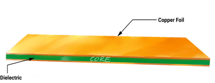
Material Selection
PCB material significantly impacts performance:
- Low-loss dielectrics: Required for Gen3 and above (Df < 0.01 typical)
- Common materials:
- FR4 for Gen1/Gen2
- Megtron 6, Nelco 4000-13 for Gen3+
- Rogers materials for extreme high-speed
- Consistency: Ensure consistent dielectric properties across the board
Connector and Package Considerations
7. Connector Implementation
- Impedance matching: Choose connectors with impedance matching the PCB
- Pinout arrangement: Follow manufacturer recommendations for pin assignments
- Grounding: Ensure proper grounding of connector shells
8. Package Routing
- Escape routing: Fanout patterns should maintain symmetry
- Ball grid arrays: Use via-in-pad or microvia technology for dense packages
- Dielectric thickness: Thin dielectrics help with escape routing
Power Delivery Network (PDN) Design
A robust PDN is critical for signal integrity:
- Decoupling capacitors: Place close to power pins (0402 or smaller recommended)
- Power plane capacitance: Use thin dielectrics between power/ground planes
- VRM placement: Position voltage regulators close to the PCIe device
- Impedance target: Typically < 1mΩ impedance up to 1GHz
Simulation and Verification
Always verify designs through simulation:
- Pre-layout simulation: Determine acceptable routing topologies
- Post-layout simulation: Verify signal integrity and power integrity
- Key analyses:
- Time-domain reflectometry (TDR)
- Eye diagram analysis
- Insertion loss/return loss
- Crosstalk analysis
Manufacturing Considerations
Ensure designs are manufacturable:
- Tolerances: Account for ±10% impedance variation in manufacturing
- Stackup tolerance: Dielectric thickness can vary ±10%
- Surface finishes: ENIG or immersion silver preferred over HASL
- Testability: Include test points for validation
PCIe Generation-Specific Guidelines
PCIe Gen1/Gen2 (2.5/5 GT/s)
- FR4 material generally acceptable
- Relaxed length matching requirements
- Standard via technology sufficient
PCIe Gen3 (8 GT/s)
- Low-loss materials recommended
- Tighter impedance control required
- Consider back-drilling for long vias
PCIe Gen4 (16 GT/s)
- Ultra-low-loss materials required
- Strict length matching (< 1 mil)
- Back-drilling typically required
- Advanced via technologies (uVias, filled vias)
PCIe Gen5 (32 GT/s) and Beyond
- Specialized materials essential
- PAM4 signaling requires exceptional signal integrity
- Consider co-design with package and connector
- May require retimers for longer channels
Common Pitfalls to Avoid
- Insufficient ground return paths: Creates impedance discontinuities
- Improper via transitions: Major source of reflections
- Excessive length mismatches: Causes intersymbol interference
- Routing over plane splits: Destroys reference plane continuity
- Inadequate decoupling: Leads to power supply noise coupling
- Poor connector implementation: Negates good board routing
- Ignoring manufacturing tolerances: Causes impedance variations
Conclusion
Proper high-speed routing for PCI Express requires attention to numerous details from impedance control and differential pair routing to via optimization and power delivery. As data rates continue increasing with each new PCIe generation, the margin for error decreases significantly. By following these guidelines—maintaining consistent impedance, minimizing discontinuities, controlling lengths, and managing reference planes—designers can achieve robust PCI Express implementations that meet performance specifications. Always remember to verify designs through simulation and measurement, as theoretical calculations alone cannot account for all real-world effects in high-speed digital designs.
The implementation details will vary based on specific PCIe generation, board stackup, and manufacturing capabilities, but the fundamental principles outlined here provide a solid foundation for successful high-speed PCI Express PCB design.