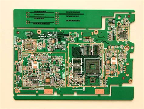
High speed pcb traces
High-speed PCB traces are used in electronic circuits to transmit signals at high frequencies, typically above 50 MHz.
These traces are designed to minimize signal distortion and noise, and to maintain signal integrity.
There are several techniques used to design high-speed PCB traces, including:
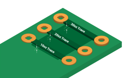
1. Controlled impedance:
The trace width and spacing are carefully controlled to maintain a consistent impedance along the length of the trace.
2. Differential signaling:
Two traces are used to transmit a signal, with one trace carrying the signal and the other carrying its inverse.
This helps to minimize noise and interference.
3. Ground planes:
A ground plane is placed adjacent to the signal trace to provide a low-impedance return path for the signal.
4. Serpentine routing:
The trace is routed in a serpentine pattern to increase its length and reduce its capacitance, which can improve signal quality.
5. Via stitching:
Multiple vias are placed along the trace to provide a low-impedance connection to the ground plane.
Overall, high-speed PCB trace design is a complex and specialized field that requires careful consideration of many factors,
including signal frequency, trace length, and board layout.

the role of high speed pcb traces
High speed PCB traces play a critical role in the performance of electronic devices and systems.
They are responsible for carrying high-frequency signals between components and ensuring that the signals arrive at their destination with minimal distortion and delay.
High-speed PCB traces must be designed with careful attention to their width, length,
and impedance to ensure that they can carry signals at the required frequency without introducing noise or signal loss.
They must also be routed in a way that minimizes crosstalk and interference from other signals on the board.
In addition to their role in signal transmission, high-speed PCB traces can also affect the overall reliability and durability of electronic devices.
Poorly designed traces can lead to signal integrity issues, which can cause errors or even system failures.
Overall, the design and implementation of high-speed PCB traces is a critical aspect of electronic system design,
and requires careful consideration and expertise to ensure optimal performance and reliability.

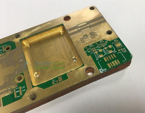
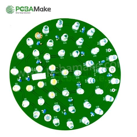
high speed pcb via
A high-speed PCB via is a type of via that is designed to handle high-frequency signals without causing any signal degradation or loss.
These vias are typically smaller in size and have a shorter length than regular vias, which helps to reduce signal reflections and improve signal integrity.
High-speed PCB vias are also often placed strategically in the PCB layout to minimize the length of the signal path and reduce the risk of interference from other components.
Some common types of high-speed PCB vias include blind vias, buried vias, and microvias.

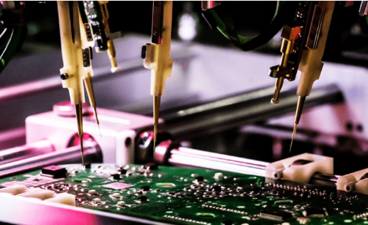
How to pass high-speed PCB
To pass high-speed PCB, there are several important considerations that must be taken into account during the design and layout process.
Here are some key steps to follow:
1. Choose the right materials:
High-speed PCBs require materials with low dielectric constant and loss tangent to minimize signal loss and distortion.
FR-4 is a common choice for low-speed PCBs, but for high-speed PCBs, materials like Rogers or Isola are recommended.
2. Minimize signal path length:
The longer the signal path, the more likely it is to experience signal degradation.
By minimizing the signal path length, you can reduce the risk of signal loss and distortion.
3. Use controlled impedance:
High-speed signals require controlled impedance to maintain signal integrity.
This means that the trace width, spacing, and dielectric thickness must be carefully calculated to match the required impedance.
4. Place vias carefully:
Vias can cause signal reflections and impedance mismatches, so they should be placed carefully to minimize their impact on the signal.
Blind vias and buried vias can be used to reduce the number of vias and minimize their impact.
5. Use proper termination techniques:
High-speed signals require proper termination to prevent reflections and signal distortion.
Techniques like series termination, parallel termination, and AC termination can be used to ensure proper signal termination.
By following these steps, you can design and layout a high-speed PCB that passes signal with minimal loss and distortion.