High speed usb pcb layout
Optimizing Trace Widths for High-Speed USB PCB Layout
When designing a high-speed USB PCB layout, one of the critical aspects to consider is the optimization of trace widths. Properly optimized trace widths are essential for maintaining signal integrity, minimizing electromagnetic interference (EMI), and ensuring reliable data transmission. The process of optimizing trace widths involves a careful balance of electrical and physical design parameters, which can significantly impact the overall performance of the USB interface.
To begin with, it is important to understand the role of trace width in high-speed USB PCB layouts.
Trace width directly influences the impedance of the signal path, which is a crucial factor in high-speed signal transmission. Impedance mismatches can lead to signal reflections, which degrade signal quality and can cause data errors. Therefore, maintaining a consistent and appropriate trace width is vital for achieving the desired impedance and ensuring signal integrity.
One of the primary considerations in optimizing trace widths is the characteristic impedance of the USB traces.
For high-speed USB applications, such as USB 3.0 and USB 3.1, the characteristic impedance is typically specified to be 90 ohms differential. To achieve this, designers must carefully calculate the trace width and spacing based on the PCB stack-up, which includes the dielectric material properties and the distance between the signal layers and the reference planes. Utilizing impedance calculators or simulation tools can aid in determining the optimal trace width and spacing to meet the required impedance specifications.
In addition to impedance control, the trace width also affects the current-carrying capacity and thermal performance of the PCB.
High-speed USB signals can generate significant amounts of heat, especially in densely packed designs. Wider traces can help dissipate heat more effectively, reducing the risk of thermal-related issues. However, increasing the trace width can also lead to increased parasitic capacitance, which can adversely affect signal integrity. Therefore, designers must strike a balance between thermal management and signal performance when determining the trace width.
Another factor to consider is the manufacturing tolerances of the PCB fabrication process.
Variations in trace width and spacing can occur due to etching and plating processes, which can impact the final impedance and signal performance. To mitigate these variations, designers should work closely with PCB manufacturers to understand their capabilities and tolerances. Specifying tighter tolerances and incorporating design-for-manufacturability (DFM) guidelines can help ensure that the fabricated PCB meets the intended design specifications.
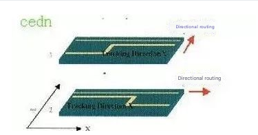
Furthermore, the layout of high-speed USB traces should minimize the length of signal paths and avoid unnecessary bends or vias.
Long signal paths and excessive bends can introduce additional inductance and capacitance, leading to signal degradation. When bends are necessary, using gradual curves instead of sharp angles can help maintain signal integrity. Additionally, minimizing the use of vias, which introduce discontinuities in the signal path, can further enhance signal performance.
In conclusion, optimizing trace widths for high-speed USB PCB layouts is a multifaceted process that requires careful consideration of impedance control, thermal management, manufacturing tolerances, and signal path layout. By meticulously balancing these factors, designers can achieve reliable and high-performance USB interfaces that meet the stringent requirements of modern high-speed applications. Employing advanced simulation tools and collaborating closely with PCB manufacturers can further enhance the design process, ensuring that the final product delivers optimal performance and reliability.
Minimizing Crosstalk in High-Speed USB PCB Designs
Minimizing crosstalk in high-speed USB PCB designs is a critical aspect of ensuring signal integrity and overall performance. As USB technology continues to advance, with speeds reaching up to 10 Gbps in USB 3.1 and beyond, the challenges associated with crosstalk become increasingly significant. Crosstalk, which refers to the unwanted coupling of signals between adjacent traces, can lead to data corruption, increased error rates, and degraded performance. Therefore, understanding and implementing effective strategies to minimize crosstalk is essential for any high-speed USB PCB design.
One of the primary methods to reduce crosstalk is to maintain adequate spacing between signal traces.
By increasing the distance between adjacent traces, the electromagnetic interference (EMI) that causes crosstalk can be significantly reduced. This is particularly important for differential pairs, which are commonly used in high-speed USB designs. Differential pairs should be routed with consistent spacing and should be kept as close together as possible to ensure that any induced noise affects both lines equally, thereby canceling out the interference.
In addition to spacing, the use of ground planes is another effective strategy for minimizing crosstalk.
Ground planes provide a low-impedance return path for signals, which helps to contain and isolate electromagnetic fields. By placing a continuous ground plane beneath the signal layers, designers can create a controlled impedance environment that reduces the potential for crosstalk. It is also beneficial to use multiple ground planes in a multilayer PCB design, as this further enhances the isolation between signal layers.
Another important consideration is the routing of signal traces.
Avoiding parallel routing of high-speed signals over long distances can help to minimize crosstalk. When parallel routing is unavoidable, it is advisable to introduce a ground trace or plane between the signal traces to act as a shield. Additionally, using serpentine routing techniques can help to equalize the lengths of differential pairs, ensuring that any crosstalk is balanced and less likely to cause issues.
The choice of materials and stack-up configuration also plays a crucial role in minimizing crosstalk.
High-quality dielectric materials with low loss tangents can help to reduce signal attenuation and maintain signal integrity. The stack-up configuration should be carefully designed to ensure that signal layers are adequately separated by ground or power planes, which helps to isolate signals and reduce crosstalk.
Furthermore, the use of proper termination techniques is essential in high-speed USB PCB designs.
Termination resistors can help to match the impedance of the transmission line, thereby reducing reflections and minimizing crosstalk. It is important to place termination resistors as close to the source or load as possible to ensure effective impedance matching.
Finally, simulation and testing are indispensable tools in the design process.
Using simulation software to model the PCB layout and analyze potential crosstalk issues can help designers identify and address problems before physical prototyping. Once the PCB is fabricated, thorough testing using high-speed oscilloscopes and other diagnostic tools can verify that crosstalk has been minimized and that the design meets performance requirements.
In conclusion, minimizing crosstalk in high-speed USB PCB designs requires a comprehensive approach that includes careful trace spacing, the use of ground planes, strategic routing, appropriate material selection, proper termination, and rigorous simulation and testing. By implementing these strategies, designers can ensure that their high-speed USB designs achieve optimal performance and reliability.

Effective Grounding Techniques for High-Speed USB PCBs
Effective grounding techniques are paramount in the design of high-speed USB printed circuit boards (PCBs) to ensure signal integrity, minimize electromagnetic interference (EMI), and enhance overall performance. As USB technology continues to evolve, supporting higher data rates and more complex functionalities, the importance of meticulous grounding strategies cannot be overstated. To achieve optimal results, designers must consider several key aspects, including ground plane design, via placement, and the separation of analog and digital grounds.
One of the fundamental principles in high-speed USB PCB design is the implementation of a continuous ground plane.
A solid ground plane provides a low-impedance path for return currents, which is crucial for maintaining signal integrity. By minimizing the impedance, the ground plane helps to reduce noise and crosstalk between signal traces. Additionally, a continuous ground plane aids in the effective dissipation of heat, which is particularly important in high-speed applications where thermal management is a concern. To ensure the ground plane remains uninterrupted, designers should avoid placing signal traces or components that could create gaps or splits in the plane.
Another critical aspect of grounding in high-speed USB PCBs is the strategic placement of vias.
Vias are used to connect different layers of the PCB, and their placement can significantly impact the performance of the ground plane. To minimize inductance and ensure a low-impedance path, it is advisable to place multiple ground vias around high-speed signal traces and near connectors. This practice helps to maintain a robust ground connection and reduces the potential for signal degradation. Furthermore, stitching vias, which are placed at regular intervals along the edge of the ground plane, can enhance the overall integrity of the ground plane by providing additional paths for return currents.
In high-speed USB PCB design, the separation of analog and digital grounds is another essential consideration.
Analog and digital circuits have different noise characteristics, and their interaction can lead to performance issues if not properly managed. By separating the analog and digital grounds, designers can isolate noise sources and prevent them from interfering with each other. This separation can be achieved by creating distinct ground planes for analog and digital sections of the PCB and connecting them at a single point, often referred to as a star ground. This approach helps to minimize noise coupling and ensures that each section of the PCB operates within its optimal noise environment.
Moreover, the placement of decoupling capacitors plays a vital role in effective grounding.
Decoupling capacitors are used to filter out high-frequency noise and provide a stable power supply to the components. Placing these capacitors close to the power pins of integrated circuits (ICs) and ensuring a low-impedance connection to the ground plane can significantly enhance the performance of the PCB. The use of multiple capacitors with different values can provide a broader frequency range of noise suppression, further improving the overall stability of the system.
In conclusion, effective grounding techniques are essential for the successful design of high-speed USB PCBs. By implementing a continuous ground plane, strategically placing vias, separating analog and digital grounds, and optimizing the placement of decoupling capacitors, designers can ensure signal integrity, minimize EMI, and enhance the overall performance of their designs. As USB technology continues to advance, adhering to these grounding principles will become increasingly important in meeting the demands of high-speed applications.
Best Practices for Differential Pair Routing in High-Speed USB Layouts
In the realm of high-speed USB printed circuit board (PCB) design, the meticulous routing of differential pairs is paramount to ensuring signal integrity and optimal performance. Differential pairs, which consist of two complementary signals, are essential in minimizing electromagnetic interference (EMI) and crosstalk, thereby maintaining the fidelity of high-speed data transmission. To achieve this, several best practices must be adhered to during the layout process.
Firstly, it is crucial to maintain consistent trace geometry throughout the routing of differential pairs.
This involves ensuring that the traces are of equal length and have a uniform width and spacing. Any deviation in these parameters can lead to signal skew, where one signal arrives before the other, potentially causing data corruption. To mitigate this, designers should employ length matching techniques, such as serpentine routing, to equalize the path lengths of the differential pairs.
Moreover, the impedance of the differential pairs must be controlled and matched to the characteristic impedance of the USB standard, typically 90 ohms differential.
This can be achieved by carefully selecting the trace width, spacing, and the dielectric material of the PCB. Impedance calculators and field solver tools are invaluable in this regard, providing precise calculations to ensure that the differential pairs meet the required impedance specifications.
Another critical aspect is the routing topology.
Differential pairs should be routed as closely coupled pairs to maximize the benefits of differential signaling. This close coupling helps to cancel out common-mode noise and reduces susceptibility to external EMI. Additionally, it is advisable to avoid routing differential pairs over split planes or across plane transitions, as this can introduce impedance discontinuities and degrade signal integrity. Instead, differential pairs should be routed over continuous ground planes to provide a stable reference and minimize impedance variations.
Furthermore, the use of vias in differential pair routing should be minimized.
Vias introduce inductance and capacitance, which can disrupt the impedance and cause signal reflections. If vias are unavoidable, it is essential to use them symmetrically on both traces of the differential pair to maintain balance. Additionally, back-drilling can be employed to remove the unused portion of the via, thereby reducing its impact on signal integrity.
In addition to these physical layout considerations, it is also important to pay attention to the placement of components.
High-speed USB components, such as connectors and transceivers, should be placed as close to each other as possible to minimize the length of the differential pairs. This reduces the potential for signal degradation and EMI. Moreover, careful consideration should be given to the placement of decoupling capacitors and other passive components to ensure that they do not interfere with the differential pairs.
Lastly, thorough simulation and testing are indispensable in the design process.
Signal integrity simulation tools can help identify potential issues and allow for optimization before the PCB is fabricated. Once the PCB is manufactured, rigorous testing, including eye diagram analysis and time-domain reflectometry (TDR), should be conducted to verify that the differential pairs meet the required performance criteria.
In conclusion, the successful routing of differential pairs in high-speed USB PCB layouts hinges on a combination of precise trace geometry, controlled impedance, appropriate routing topology, minimal use of vias, strategic component placement, and comprehensive simulation and testing. By adhering to these best practices, designers can ensure robust signal integrity and reliable high-speed data transmission in their USB designs.