High voltage pcb layout
Best Practices For High Voltage PCB Layout Design
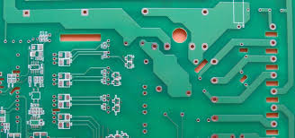
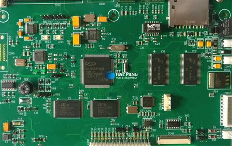
Designing a high voltage printed circuit board (PCB) requires meticulous attention to detail and adherence to best practices to ensure safety, reliability, and performance.
One of the primary considerations in high voltage PCB layout design is the spacing between conductive elements.
Adequate clearance and creepage distances are essential to prevent electrical arcing and ensure insulation integrity. Clearance refers to the shortest distance through the air between two conductive parts, while creepage is the shortest path along the surface of an insulating material. Both distances must comply with industry standards and regulations, such as those outlined by the International Electrotechnical Commission (IEC).
In addition to spacing, the choice of materials plays a crucial role in high voltage PCB design.
The dielectric properties of the substrate material must be carefully selected to withstand high voltages without breaking down. Materials with high dielectric strength, such as FR4 or polyimide, are commonly used. Furthermore, the thickness of the PCB substrate can influence its ability to handle high voltages. Thicker substrates provide better insulation and reduce the risk of dielectric breakdown.
Another critical aspect is the layout of the ground plane.
A well-designed ground plane can significantly reduce electromagnetic interference (EMI) and improve the overall performance of the PCB. It is advisable to use a continuous ground plane and avoid splitting it into multiple sections. This approach minimizes the potential for ground loops and ensures a low-impedance path for return currents. Additionally, placing the ground plane on an internal layer of the PCB can provide better shielding and reduce the risk of high voltage arcing.
Thermal management is also a key consideration in high voltage PCB design.
High voltage components can generate significant amounts of heat, which must be effectively dissipated to prevent damage and ensure reliable operation. Incorporating thermal vias, heat sinks, and adequate copper thickness can help manage heat dissipation. Moreover, careful placement of high power components can prevent localized hotspots and improve overall thermal performance.
Signal integrity is another important factor in high voltage PCB layout design.
High voltage signals can be susceptible to noise and crosstalk, which can degrade performance and lead to malfunction. To mitigate these issues, it is essential to use proper routing techniques, such as maintaining consistent trace widths and avoiding sharp bends. Additionally, differential pair routing and controlled impedance traces can help maintain signal integrity and reduce noise.
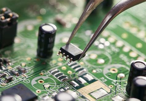
Component selection and placement are equally important in high voltage PCB design.
Components must be rated for the appropriate voltage levels and should be placed to minimize the risk of arcing and short circuits. It is advisable to keep high voltage components away from low voltage circuitry to prevent interference and potential damage. Furthermore, using conformal coatings can provide an additional layer of protection against environmental factors, such as moisture and dust, which can compromise the performance of high voltage PCBs.
In conclusion, designing a high voltage PCB requires a comprehensive understanding of various factors, including spacing, material selection, ground plane layout, thermal management, signal integrity, and component placement. By adhering to best practices and industry standards, designers can create high voltage PCBs that are safe, reliable, and efficient. The meticulous attention to detail in each aspect of the design process ensures that the final product meets the stringent requirements of high voltage applications.
Safety Considerations In High Voltage PCB Layout
When designing high voltage printed circuit boards (PCBs), safety considerations are paramount to ensure both the functionality and reliability of the system, as well as the protection of users and equipment. High voltage PCBs are used in various applications, including power supplies, industrial equipment, and medical devices, where the potential for electrical hazards is significant. Therefore, meticulous attention to detail is required to mitigate risks associated with high voltage operations.
One of the primary safety considerations in high voltage PCB layout is the establishment of adequate clearance and creepage distances.
Clearance refers to the shortest path between two conductive parts through the air, while creepage is the shortest path along the surface of an insulating material. These distances are critical in preventing electrical arcing and ensuring insulation integrity. The required clearance and creepage distances depend on the operating voltage, environmental conditions, and the type of insulation material used. Adhering to industry standards, such as those set by the International Electrotechnical Commission (IEC), helps in determining the appropriate distances to maintain.
In addition to clearance and creepage, the choice of materials plays a crucial role in high voltage PCB safety.
The dielectric strength of the PCB substrate must be sufficient to withstand the operating voltage without breaking down. Common materials like FR4 may not be suitable for very high voltage applications, necessitating the use of specialized high voltage laminates. Furthermore, the insulation resistance of the materials should be high to minimize leakage currents, which can lead to power loss and potential hazards.
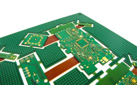
Another important aspect is the layout of high voltage traces.
These traces should be routed with care to avoid sharp bends and corners, which can concentrate electric fields and increase the risk of dielectric breakdown. Smooth, gradual curves are preferred to distribute the electric field more evenly. Additionally, high voltage traces should be kept away from low voltage circuits to prevent accidental coupling and potential damage to sensitive components. Shielding and isolation techniques, such as the use of guard rings and barriers, can further enhance safety by providing additional layers of protection.
Thermal management is also a critical consideration in high voltage PCB design.
High voltage components often generate significant heat, which can affect the performance and longevity of the PCB. Effective heat dissipation methods, such as the use of thermal vias, heat sinks, and proper ventilation, are essential to maintain safe operating temperatures. Overheating can compromise insulation materials and lead to catastrophic failures, making thermal management an integral part of the safety strategy.
Moreover, the implementation of protective devices is essential in high voltage PCB layouts.
Components such as fuses, varistors, and transient voltage suppression (TVS) diodes can protect the circuit from overvoltage conditions and transient spikes. These devices act as safeguards, preventing excessive voltage from reaching sensitive parts of the circuit and thereby reducing the risk of damage and fire hazards.
Finally, thorough testing and validation are indispensable to ensure the safety of high voltage PCBs.
High potential (hipot) testing, insulation resistance testing, and partial discharge testing are some of the methods used to verify the integrity of the insulation and the overall robustness of the PCB design. Regular maintenance and inspection are also necessary to identify and address any potential issues that may arise during the operational life of the PCB.
In conclusion, safety considerations in high voltage PCB layout encompass a range of factors, including clearance and creepage distances, material selection, trace routing, thermal management, protective devices, and rigorous testing. By meticulously addressing these aspects, designers can create high voltage PCBs that are not only efficient and reliable but also safe for users and equipment.
Material Selection For High Voltage PCB Applications
When designing high voltage printed circuit boards (PCBs), the selection of appropriate materials is paramount to ensure both performance and safety. High voltage applications demand materials that can withstand significant electrical stress, maintain structural integrity, and provide reliable insulation. Consequently, the choice of substrate, dielectric materials, and conductive elements must be meticulously considered.
To begin with, the substrate material forms the foundation of the PCB and plays a crucial role in its overall performance.
For high voltage applications, FR-4, a widely used substrate in standard PCBs, may not always be suitable due to its limited dielectric strength. Instead, materials such as polyimide, ceramic-filled PTFE, or high-performance laminates like Rogers materials are often preferred. These substrates offer superior dielectric properties, higher thermal stability, and better mechanical strength, making them ideal for high voltage environments.
In addition to the substrate, the dielectric material used between the conductive layers is equally important.
The dielectric constant and breakdown voltage of the material must be carefully evaluated to ensure it can handle the high voltage without degrading. Materials such as Teflon (PTFE), ceramic-filled composites, and certain high-grade epoxies are commonly used due to their excellent insulating properties and high dielectric strength. These materials help in minimizing the risk of dielectric breakdown, which can lead to catastrophic failures in high voltage circuits.
Furthermore, the choice of conductive materials is critical in high voltage PCB design.
Copper is the standard choice for conductors due to its excellent electrical conductivity and relatively low cost. However, in high voltage applications, the thickness of the copper traces must be increased to handle the higher current loads and to reduce the risk of arcing. Additionally, surface finishes such as gold or silver plating can be employed to enhance conductivity and protect against oxidation, which can compromise the performance of the PCB over time.
Moreover, the layout and spacing of the conductive traces must be carefully designed to prevent electrical arcing and ensure adequate insulation.
The use of wider trace widths and increased spacing between traces helps in mitigating the risk of short circuits and arcing. Additionally, incorporating techniques such as conformal coating or potting can provide an extra layer of insulation and protection against environmental factors such as moisture and dust, which can further enhance the reliability of high voltage PCBs.
Transitioning to the aspect of thermal management,
high voltage PCBs often generate significant amounts of heat, which must be effectively dissipated to maintain performance and prevent damage. Materials with high thermal conductivity, such as aluminum or copper-clad substrates, can be used to facilitate efficient heat dissipation. Additionally, incorporating thermal vias and heat sinks into the PCB design can further aid in managing thermal loads and ensuring the longevity of the board.
In conclusion, the selection of materials for high voltage PCB applications is a multifaceted process that requires careful consideration of various factors including dielectric strength, thermal stability, and electrical conductivity. By choosing appropriate substrates, dielectric materials, and conductive elements, and by implementing effective layout and thermal management strategies, designers can create high voltage PCBs that are both reliable and safe. This meticulous approach to material selection not only enhances the performance of the PCB but also ensures its durability in demanding high voltage environments.
Common Mistakes To Avoid In High Voltage PCB Layout
Designing a high voltage PCB layout requires meticulous attention to detail and a thorough understanding of the principles governing high voltage circuits. One common mistake is underestimating the importance of clearance and creepage distances. These distances are critical in preventing arcing and ensuring the safety and reliability of the PCB. Designers often overlook the need to adhere to industry standards, such as IPC-2221, which provides guidelines for these distances based on the operating voltage. Failing to maintain adequate clearance and creepage can lead to catastrophic failures, including short circuits and component damage.
Another frequent error is the improper placement of components.
High voltage components should be strategically placed to minimize the risk of arcing and to ensure efficient heat dissipation. Placing high voltage components too close to low voltage components can result in interference and potential damage. Additionally, designers should avoid placing components near the edges of the PCB, as this can increase the risk of arcing and reduce the overall robustness of the design.
Inadequate grounding is another pitfall in high voltage PCB layout.
A solid grounding strategy is essential for the stability and performance of the circuit. Designers often make the mistake of using a single ground plane for both high and low voltage sections, which can lead to noise and interference issues. Instead, it is advisable to use separate ground planes and connect them at a single point to minimize noise coupling. Furthermore, ensuring that the ground plane is continuous and free of gaps can significantly enhance the performance of the PCB.
Thermal management is another critical aspect that is often neglected.
High voltage components tend to generate significant amounts of heat, which can affect the performance and longevity of the PCB. Designers should incorporate adequate thermal vias and heat sinks to dissipate heat effectively. Ignoring thermal management can lead to overheating, which can cause components to fail prematurely and compromise the reliability of the entire system.
Trace routing is another area where mistakes are commonly made.
High voltage traces should be routed with care to avoid sharp bends and acute angles, which can create points of high electric field concentration and increase the risk of arcing. Additionally, designers should ensure that high voltage traces are adequately spaced from other traces and components to prevent interference and potential short circuits. Using wider traces for high voltage paths can also help in reducing resistance and improving the overall performance of the PCB.
Lastly, the choice of materials plays a crucial role in high voltage PCB design.
Using materials with inadequate dielectric strength can result in insulation breakdown and arcing. Designers should select materials that can withstand the operating voltage and environmental conditions of the application. Additionally, conformal coatings can be applied to provide an extra layer of insulation and protection against moisture and contaminants.
In conclusion, avoiding common mistakes in high voltage PCB layout requires a comprehensive understanding of the principles and best practices involved. By paying close attention to clearance and creepage distances, component placement, grounding strategies, thermal management, trace routing, and material selection, designers can create robust and reliable high voltage PCBs. Ensuring adherence to industry standards and guidelines is essential in achieving a successful design that meets the required performance and safety criteria.