High voltage Print Circuit Board (HV PCBs)
High Voltage Printed Circuit Boards (HV PCBs): Design, Materials, and Applications
Introduction to HV PCBs
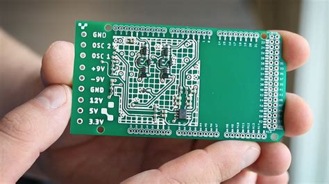
High Voltage Printed Circuit Boards (HV PCBs) represent a specialized segment of the electronics manufacturing industry designed to handle significantly higher voltages than standard PCBs. While conventional PCBs typically operate at voltages below 50V, HV PCBs are engineered to withstand voltages ranging from hundreds to thousands of volts, with some specialized designs handling tens of thousands of volts.
The growing demand for HV PCBs stems from their critical applications in power electronics, renewable energy systems, medical equipment, industrial automation, and electric vehicles. As these industries continue to expand, the importance of reliable high voltage circuit boards becomes increasingly apparent.
Key Design Considerations for HV PCBs
1. Creepage and Clearance Distances
The fundamental challenge in HV PCB design lies in managing the increased risk of arcing and dielectric breakdown. Two critical concepts govern this aspect:
- Clearance: The shortest air path between two conductive elements
- Creepage: The shortest path along the surface of the insulating material between conductors
Design standards such as IPC-2221 and IEC 60950 provide guidelines for minimum clearance and creepage distances based on:
- Operating voltage
- Pollution degree (environmental conditions)
- Material group (CTI – Comparative Tracking Index)
For example, at 1000V in a pollution degree 2 environment, the minimum clearance might be 6.3mm, while the creepage distance could range from 8mm to 12.5mm depending on the material group.
2. Dielectric Material Selection
The choice of dielectric material significantly impacts HV PCB performance. Key properties to consider include:
- Dielectric Strength: Typically measured in V/mil, determines how much voltage the material can withstand before breaking down
- Comparative Tracking Index (CTI): Measures the material’s resistance to surface tracking (higher is better for HV applications)
- Thermal Stability: Important as temperature affects dielectric properties
- Moisture Absorption: Water can dramatically reduce dielectric strength
Common HV PCB materials include:
- FR-4 (modified versions for HV)
- Polyimide
- PTFE (Teflon)
- Ceramic-filled laminates
- Specialty high-performance materials like Megtron, Isola 370HR, or Rogers RO4350B
3. Copper Thickness and Trace Geometry
HV PCBs often require:
- Thicker copper (2oz to 6oz or more) to handle higher currents
- Wider traces to reduce current density and heating
- Rounded trace corners to minimize corona discharge
- Proper via design to prevent arcing through plated through-holes
4. Layer Stackup and Insulation
Multi-layer HV PCBs require careful stackup design:
- Increased core thickness between high voltage layers
- Proper arrangement of high and low voltage layers
- Use of buried or blind vias to control potential differences
- Consideration of partial discharge (corona) effects at very high voltages
5. Solder Mask and Conformal Coatings
Special considerations for HV applications:
- Thicker solder mask applications
- High dielectric strength conformal coatings (silicone, polyurethane, or parylene)
- Complete coverage of all conductive surfaces
- Avoidance of pinholes or voids in coatings
Manufacturing Processes for HV PCBs
1. Material Preparation
HV PCBs begin with careful material selection and preparation:
- Verification of dielectric material specifications
- Controlled storage to prevent moisture absorption
- Pre-baking if necessary to remove moisture
2. Precision Etching
The etching process requires:
- Tight control of trace width and spacing
- Minimization of undercutting
- Smooth edge quality (no burrs or rough edges)
3. Drilling and Hole Preparation
Critical aspects include:
- Clean, debris-free hole walls
- Proper desmearing for multilayer boards
- Careful via plating to ensure uniform thickness
- Possible filling of vias with dielectric material
4. Surface Finishes
Common HV PCB surface finishes:
- Immersion silver
- Electroless nickel immersion gold (ENIG)
- Organic solderability preservatives (OSP)
- Hard gold for edge connectors
5. Quality Control and Testing
Rigorous testing protocols for HV PCBs:
- Automated optical inspection (AOI)
- High voltage dielectric withstand testing (HiPot)
- Insulation resistance testing
- Partial discharge testing for very high voltage applications
Applications of HV PCBs
1. Power Electronics
- Switch-mode power supplies
- Inverters and converters
- Motor drives
- Power distribution systems
2. Renewable Energy Systems
- Solar inverters
- Wind turbine control systems
- Battery management systems for grid storage
3. Medical Equipment
- X-ray machines
- MRI systems
- Electrosurgical units
- Medical imaging devices
4. Industrial Equipment
- Plasma generators
- Industrial lasers
- High voltage test equipment
- Power quality monitoring systems
5. Transportation
- Electric vehicle charging systems
- Traction inverters for EVs
- Railway power systems
- Aerospace power distribution
Emerging Trends in HV PCB Technology
1. Higher Voltage Capabilities
As industries push for more efficient power transmission and conversion, demand grows for PCBs capable of handling:
- 10kV+ in compact designs
- Medium voltage applications (1kV to 35kV)
- Mixed voltage boards combining high and low voltage sections
2. Advanced Materials
Development of new materials offering:
- Higher dielectric strength
- Better thermal conductivity
- Improved partial discharge resistance
- Enhanced environmental stability
3. 3D Printed Electronics
Additive manufacturing techniques enabling:
- Complex HV insulation structures
- Integrated high voltage components
- Custom geometries for improved field management
4. Embedded Components
Integration of passive and active components within the PCB structure:
- Embedded resistors and capacitors
- Semiconductor dies in protected cavities
- Reduced interconnection distances
5. Smart Monitoring
Incorporation of:
- Built-in voltage and current sensors
- Temperature monitoring
- Partial discharge detection
- Predictive maintenance capabilities
Challenges and Future Directions
Despite significant advancements, HV PCB technology faces several challenges:
- Miniaturization vs. Safety: Balancing the demand for smaller boards with necessary safety clearances
- Thermal Management: Dissipating heat from high power components while maintaining dielectric properties
- Cost Pressures: Developing cost-effective solutions for mass-market applications like electric vehicles
- Standardization: Establishing industry-wide standards for emerging HV PCB applications
- Reliability Testing: Developing accelerated life testing methods for long-life applications
Future developments will likely focus on:
- Nanocomposite dielectric materials
- AI-assisted design tools for optimized HV layouts
- Integrated cooling solutions
- Environmentally friendly materials and processes
- Hybrid designs combining PCB and busbar technologies
Conclusion
High Voltage Printed Circuit Boards represent a critical enabling technology for modern power electronics and energy conversion systems. Their specialized design requirements, from material selection to layout considerations, set them apart from conventional PCBs. As global trends toward electrification, renewable energy, and high-efficiency power systems continue, the importance of HV PCB technology will only grow.
Engineers and designers working with HV PCBs must balance electrical, thermal, mechanical, and safety requirements to create reliable, high-performance solutions. With ongoing advancements in materials, manufacturing processes, and design methodologies, HV PCBs are poised to meet the increasingly demanding requirements of next-generation power electronics applications.
The future of HV PCB technology promises not only higher voltage capabilities in smaller form factors but also smarter, more integrated solutions that will drive innovation across multiple industries. As such, continued research and development in this field remains essential for supporting the global transition to more efficient, electrified systems.


