How are chips packaged? Introduction to chip packaging steps
Chips are the basis of all intelligence. Without chips, electronic devices are equivalent to lacking the “thinking ability” of the “brain”. In the previous article, the editor explained the common types of chip packaging. In order to enhance everyone’s understanding of chips, this article will introduce the chip packaging steps, mainly introducing the main welding methods of COB. If you are interested in chips, you may wish to continue reading.

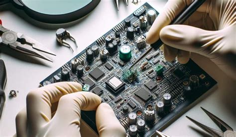
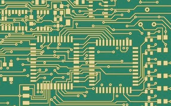
The chip on board (COB) process first covers the silicon wafer placement point on the substrate surface with thermal conductive epoxy resin (generally epoxy resin doped with silver particles), and then directly places the silicon wafer on the substrate surface, heat treats until the silicon wafer is firmly fixed on the substrate, and then uses wire welding to directly establish electrical connections between the silicon wafer and the substrate.
There are two main forms of bare chip technology: one is COB technology, and the other is flip chip technology (FlipChip). Chip on Board (COB), semiconductor chips are mounted on printed circuit boards, and the electrical connection between the chip and the substrate is achieved by wire stitching, and covered with resin to ensure reliability. Although COB is the simplest bare chip mounting technology, its packaging density is far inferior to TAB and flip chip welding technology. In the following, the editor mainly introduces the main welding methods of COB.
(1) Hot Pressing
The metal wire and the welding area are pressed together by heating and applying pressure. The principle is to make the welding area (such as AI) plastically deformed by heating and applying pressure, and at the same time destroy the oxide layer on the pressure welding interface, so that the atoms are attracted to each other to achieve the purpose of “bonding”. In addition, when the two metal interfaces are uneven, the upper and lower metals can be inlaid with each other when heated and pressed. This technology is generally used for COG chips on glass plates.
(2) Ultrasonic welding
Ultrasonic welding uses the energy generated by an ultrasonic generator. Through the transducer, under the induction of an ultra-high frequency magnetic field, it quickly expands and contracts to produce elastic vibrations, causing the splitter to vibrate accordingly. At the same time, a certain amount of pressure is applied to the splitter. Under the combined action of these two forces, the splitter drives the AI wire to quickly rub against the metallized layer (AI film) surface of the welded area, causing plastic deformation of the AI wire and the AI film surface. This deformation also destroys the oxide layer at the interface of the AI layer, allowing the two pure metal surfaces to come into close contact to achieve atomic bonding, thereby forming a weld. The main welding material is an aluminum wire welding head, which is generally wedge-shaped.
(3) Gold wire welding
Ball welding is the most representative welding technology in wire bonding, because the current semiconductor packaging diode and transistor packaging all use AU wire ball welding. Moreover, it is easy to operate, flexible, and has a firm solder joint (the welding strength of AU wire with a diameter of 25UM is generally 0.07~0.09N/point), and has no directionality. The welding speed can be as high as 15 points/second or more. Gold wire welding is also called hot (pressure) (supersonic) welding. The main bonding material is gold (AU). The wire welding head is spherical, so it is a ball welding.
COB packaging process
Step 1: Crystal expansion. Use an expansion machine to evenly expand the entire LED chip film provided by the manufacturer, so that the LED grains closely arranged on the surface of the film are pulled apart to facilitate crystal piercing.
Step 2: Back glue. Place the crystal expansion ring with the expanded crystal on the back glue machine surface with the silver paste layer scraped, and back the silver paste. Apply silver paste. Suitable for bulk LED chips. Use a glue dispenser to apply an appropriate amount of silver paste on the PCB printed circuit board.
Step 3: Put the crystal expansion ring with silver paste prepared into the crystal piercing rack, and the operator will pierce the LED chip on the PCB printed circuit board with a crystal piercing pen under a microscope.
Step 4: Put the PCB printed circuit board with the pierced crystal into a thermal cycle oven and let it stand at a constant temperature for a period of time, and take it out after the silver paste is solidified (it cannot be left for a long time, otherwise the LED chip coating will be baked yellow, that is, oxidized, which will cause difficulties in bonding). If there is LED chip bonding, the above steps are required; if only IC chip bonding is required, the above steps are cancelled
Step 5: Glue the chip. Use a glue dispenser to apply an appropriate amount of red glue (or black glue) to the IC position of the PCB printed circuit board, and then use anti-static equipment (vacuum suction pen or sub) to correctly place the IC bare chip on the red glue or black glue.
Step 6: Drying. Put the bonded bare chip into a thermal cycle oven and place it on a large flat heating plate at a constant temperature for a period of time, or it can be cured naturally (for a longer time).
Step 7: Bonding (wire bonding). Use an aluminum wire bonding machine to bridge the chip (LED crystal or IC chip) with the corresponding pad aluminum wire on the PCB board, that is, the inner lead welding of COB.
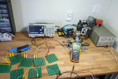
Step 8: Pre-test. Use special detection tools (there are different equipment for COBs with different uses, the simplest one is a high-precision voltage-stabilized power supply) to detect the COB board and rework the unqualified boards.
Step 9: Glue dispensing. Use a dispensing machine to apply the prepared AB glue to the bonded LED die in an appropriate amount, and the IC is encapsulated with black glue, and then the appearance is encapsulated according to customer requirements.
Step 10: Curing. Put the encapsulated PCB printed circuit board into a thermal cycle oven and keep it at a constant temperature. Different drying times can be set according to requirements.
Step 11: Post-test. Use a special detection tool to test the electrical performance of the encapsulated PCB printed circuit board to distinguish between good and bad.
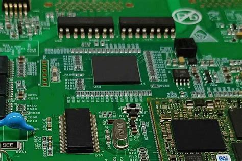
Compared with other packaging technologies, COB technology is cheap (only about 1/3 of the same chip), saves space, and has mature technology. However, no new technology can be perfect when it first appears. COB technology also has the disadvantages of needing to equip a separate welding machine and encapsulation machine, sometimes not keeping up with the speed, and PCB patch has more stringent environmental requirements and cannot be repaired.
Some chip-on-board (CoB) layouts can improve IC signal performance because they remove most or all of the packaging, that is, most or all of the parasitic devices. However, there may be some performance issues with these technologies. In all of these designs, the substrate may not be well connected to VCC or ground due to the lead frame sheet or BGA logo. Possible problems include coefficient of thermal expansion (CTE) problems and poor substrate connection.
The above is the “chip” related content brought by the editor this time. Through this article, I hope everyone has a certain understanding of the chip packaging steps. If you like this article, you may wish to continue to pay attention to our website. The editor will bring more exciting content later. Finally, thank you very much for reading, have a nice day!