How are metal core pcb lamination
How are metal core pcb lamination
Metal core printed circuit boards (PCBs) have become increasingly popular in various industries due to their superior thermal management capabilities. These PCBs are particularly advantageous in applications where heat dissipation is critical, such as in LED lighting, power supplies, and automotive electronics.
lamination process of metal core PCBs is a crucial step that ensures the structural integrity and performance of the final product. Understanding this process requires a detailed examination of the materials involved, the steps taken during lamination, and the benefits that result from this meticulous procedure.
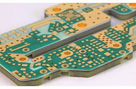
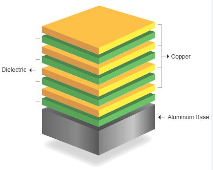
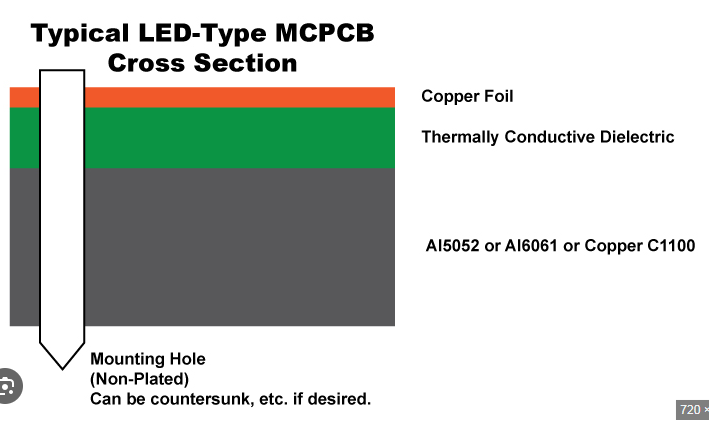
To begin with, metal core PCBs typically consist of a metal base layer, an insulating layer, and a copper circuit layer.
The metal base, often made of aluminum or copper, serves as the foundation and provides excellent thermal conductivity. The insulating layer, usually composed of a thermally conductive dielectric material, electrically isolates the metal base from the copper circuit layer while allowing heat to pass through efficiently. The copper circuit layer, which forms the electrical pathways, is laminated onto the insulating layer.
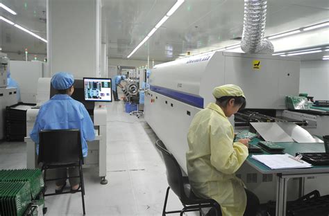
The lamination process starts with the preparation of the metal base.
This involves cleaning and treating the surface to ensure it is free from contaminants and oxidation. A clean surface is essential for achieving a strong bond between the layers. Following this, the insulating layer is applied. This layer is typically a pre-preg material, which is a fiberglass cloth impregnated with a resin that has not yet fully cured. The pre-preg material is carefully placed onto the metal base, ensuring even coverage and alignment.
Next, the copper foil, which will form the circuit layer, is placed on top of the insulating layer.
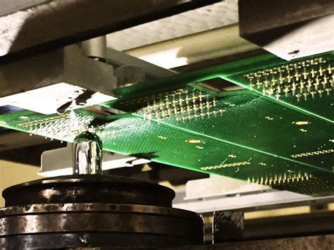
The entire stack is then subjected to heat and pressure in a lamination press. The application of heat causes the resin in the pre-preg material to flow and fill any gaps, while the pressure ensures that the layers are tightly bonded together. This step is critical as it determines the mechanical strength and thermal performance of the PCB. The temperature and pressure must be precisely controlled to avoid defects such as delamination or voids.
Once the lamination process is complete, the laminated panel undergoes a series of post-lamination processes.
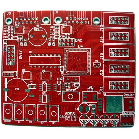
include drilling, where holes are created for electrical connections and mounting purposes, and etching, where the copper layer is patterned to form the desired circuit layout. The panel may also undergo additional treatments such as surface finishing and solder mask application to enhance its durability and functionality.
The benefits of metal core PCB lamination are manifold.
The primary advantage is improved thermal management, which is crucial for maintaining the performance and longevity of electronic components. By efficiently dissipating heat, metal core PCBs help prevent overheating and reduce the risk of thermal damage. Additionally, the robust construction of these PCBs enhances their mechanical stability, making them suitable for use in harsh environments.
In conclusion, the lamination of metal core PCBs is a sophisticated process that involves careful preparation, precise control of heat and pressure, and meticulous post-lamination treatments. This process not only ensures the structural integrity of the PCB but also significantly enhances its thermal management capabilities. As electronic devices continue to evolve and demand higher performance, the role of metal core PCBs and their lamination process will undoubtedly become even more critical in meeting these challenges.
Step-by-Step Guide To Metal Core PCB Lamination Process
The process of metal core PCB lamination is a meticulous and intricate procedure that requires precision and expertise. It begins with the selection of appropriate materials, which typically include a metal core, such as aluminum or copper, and various layers of dielectric and conductive materials. The choice of metal core is crucial as it provides the necessary thermal conductivity and mechanical stability for the PCB.
Once the materials are selected, the first step involves preparing the metal core.
This preparation includes cleaning and treating the surface to ensure it is free from contaminants and oxidation. A clean surface is essential for achieving a strong bond between the metal core and the subsequent layers. Following this, a dielectric layer is applied to the metal core. This layer acts as an insulator, preventing electrical shorts and ensuring the proper functioning of the PCB.
The next phase involves the application of the copper foil, which serves as the conductive layer.
The copper foil is carefully aligned and laminated onto the dielectric layer using heat and pressure. This process, known as hot pressing, ensures that the copper foil adheres firmly to the dielectric layer, creating a uniform and reliable conductive surface. The temperature and pressure parameters must be meticulously controlled to avoid any defects or inconsistencies in the lamination.
After the copper foil is laminated, the PCB undergoes a drilling process.
Precision drilling machines are used to create holes and vias, which are essential for establishing electrical connections between different layers of the PCB. The accuracy of this drilling process is paramount, as any misalignment can lead to faulty connections and compromised performance.
Following the drilling process, the PCB is subjected to a series of cleaning and desmearing steps.
These steps are crucial for removing any debris or residues left from the drilling process, ensuring that the holes and vias are clean and ready for plating. The next step involves the electroplating of the drilled holes and vias with copper. This electroplating process creates a conductive path through the holes, enabling electrical connections between the different layers of the PCB.
Once the electroplating is complete, the PCB undergoes a patterning process.
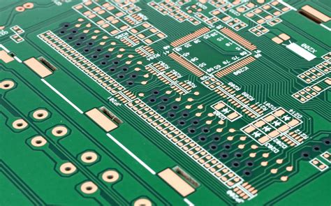
This involves applying a photoresist material to the surface of the PCB and exposing it to ultraviolet light through a photomask. The exposed areas of the photoresist harden, while the unexposed areas remain soft and can be washed away. This creates a precise pattern on the copper foil, which will form the circuit traces of the PCB.
The next step is etching, where the PCB is exposed to a chemical solution that removes the unwanted copper, leaving behind the desired circuit pattern. This etching process must be carefully controlled to ensure that the circuit traces are accurately formed and free from defects. After etching, the remaining photoresist is stripped away, revealing the final circuit pattern.
The final steps in the metal core PCB lamination process involve applying a solder mask and surface finish.
The solder mask is a protective layer that covers the circuit traces, preventing oxidation and providing insulation. The surface finish, such as HASL (Hot Air Solder Leveling) or ENIG (Electroless Nickel Immersion Gold), is applied to the exposed copper pads, ensuring good solderability and protecting the copper from corrosion.
In conclusion, the metal core PCB lamination process is a complex and precise procedure that involves multiple steps, each requiring careful attention to detail. From material selection and surface preparation to drilling, electroplating, patterning, and finishing, every stage is critical to achieving a high-quality and reliable metal core PCB.
Advantages Of Using Metal Core PCB Lamination In Electronics
Metal core printed circuit boards (PCBs) have become increasingly popular in the electronics industry due to their unique advantages, particularly in applications requiring efficient heat dissipation. The lamination process of metal core PCBs involves bonding a metal substrate, typically aluminum or copper, with dielectric and conductive layers. This process not only enhances the thermal management capabilities of the PCB but also offers several other benefits that make it an attractive choice for various electronic applications.
One of the primary advantages of using metal core PCB lamination is its superior thermal conductivity.
Traditional PCBs, which are usually made from materials like FR4, often struggle with heat dissipation, especially in high-power applications. In contrast, metal core PCBs can efficiently transfer heat away from critical components, thereby reducing the risk of overheating and improving the overall reliability of the electronic device. This is particularly beneficial in applications such as LED lighting, power supplies, and automotive electronics, where managing heat is crucial for maintaining performance and longevity.
In addition to thermal management, metal core PCB lamination also enhances the mechanical stability of the circuit board.
The metal substrate provides a robust foundation that can withstand mechanical stress and vibrations, making it ideal for use in harsh environments. This increased durability ensures that the electronic device remains functional even under challenging conditions, thereby extending its operational life. Moreover, the rigidity of the metal core helps to prevent warping and bending, which can be a common issue with traditional PCBs, especially in larger or more complex designs.
Another significant benefit of metal core PCB lamination is its potential for miniaturization.
As electronic devices continue to shrink in size, the need for compact and efficient circuit boards becomes more critical. Metal core PCBs allow for higher component density and more efficient use of space, enabling the design of smaller and more powerful electronic devices. This is particularly advantageous in industries such as consumer electronics, where there is a constant demand for more compact and portable gadgets.
Furthermore, the lamination process of metal core PCBs can also contribute to improved electrical performance.
The metal substrate can act as a ground plane, reducing electromagnetic interference (EMI) and enhancing signal integrity. This is especially important in high-frequency applications, where maintaining signal quality is essential for the proper functioning of the device. By minimizing EMI, metal core PCBs can help to ensure that electronic devices operate smoothly and without interference from external sources.
In terms of cost-effectiveness, metal core PCB lamination can offer long-term savings despite the initial higher material costs.
The improved thermal management and mechanical stability can lead to fewer failures and reduced maintenance requirements, ultimately lowering the total cost of ownership. Additionally, the enhanced performance and reliability can result in higher customer satisfaction and fewer returns, further contributing to cost savings.
In conclusion, the advantages of using metal core PCB lamination in electronics are manifold. From superior thermal conductivity and mechanical stability to potential miniaturization and improved electrical performance, metal core PCBs offer a range of benefits that make them an attractive choice for various applications. As the demand for more efficient, reliable, and compact electronic devices continues to grow, the adoption of metal core PCB lamination is likely to increase, further solidifying its position as a key technology in the electronics industry.
Common Challenges And Solutions In Metal Core PCB Lamination
Metal core printed circuit boards (PCBs) are increasingly popular in applications requiring efficient heat dissipation, such as LED lighting, power electronics, and automotive systems. However, the lamination process of metal core PCBs presents several challenges that can impact the performance and reliability of the final product. Understanding these challenges and their corresponding solutions is crucial for manufacturers aiming to produce high-quality metal core PCBs.
One of the primary challenges in metal core PCB lamination is the thermal expansion mismatch between the metal core and the dielectric materials.
Metals, such as aluminum or copper, have different coefficients of thermal expansion (CTE) compared to the dielectric layers. This discrepancy can lead to mechanical stress during thermal cycling, potentially causing delamination or cracking. To mitigate this issue, manufacturers often use dielectric materials with CTE values closely matching those of the metal core. Additionally, incorporating flexible adhesives that can absorb some of the mechanical stress can further enhance the reliability of the lamination.
Another significant challenge is ensuring uniform heat distribution during the lamination process.
Metal cores are excellent conductors of heat, which can lead to uneven temperature profiles across the PCB. This uneven heating can result in incomplete curing of the dielectric materials or warping of the metal core. To address this, manufacturers employ advanced thermal management techniques, such as using specialized lamination presses with precise temperature control and incorporating thermal pads or heat sinks to distribute heat more evenly.
The adhesion between the metal core and the dielectric layers is also a critical factor in the lamination process.
Poor adhesion can lead to delamination, reducing the mechanical integrity and thermal performance of the PCB. Surface preparation of the metal core is essential to enhance adhesion. Techniques such as chemical etching, mechanical roughening, or applying adhesion promoters can significantly improve the bond strength between the metal and dielectric layers. Furthermore, selecting high-quality dielectric materials with strong adhesive properties can also contribute to better lamination outcomes.
Void formation during lamination is another common issue that can compromise the performance of metal core PCBs.
Voids are air pockets trapped between the layers, which can act as thermal insulators and reduce the overall thermal conductivity of the PCB. To minimize void formation, manufacturers must ensure proper vacuum conditions during the lamination process. Additionally, using low-viscosity dielectric materials that can flow easily and fill gaps more effectively can help reduce the occurrence of voids.
The thickness of the dielectric layer is another aspect that requires careful consideration.
A thicker dielectric layer can provide better electrical insulation and mechanical strength but may also increase the thermal resistance, reducing the heat dissipation efficiency. Conversely, a thinner dielectric layer can enhance thermal performance but may compromise electrical insulation and mechanical integrity. Therefore, manufacturers must strike a balance between these factors, often through extensive testing and optimization, to achieve the desired performance characteristics.
In conclusion, the lamination of metal core PCBs involves addressing several challenges, including thermal expansion mismatch, heat distribution, adhesion, void formation, and dielectric thickness. By employing appropriate materials, advanced thermal management techniques, and meticulous surface preparation, manufacturers can overcome these challenges and produce high-quality metal core PCBs. As the demand for efficient thermal management in electronic devices continues to grow, ongoing research and development in lamination processes will be essential to meet the evolving needs of the industry.