How to Analyze PCB Microsections: A Comprehensive Guide
Introduction
Printed Circuit Board (PCB) microsection analysis, also known as cross-sectioning or metallographic preparation, is a critical technique used in PCB manufacturing, quality control, and failure analysis. By examining a microsection of a PCB, engineers can evaluate plating quality, layer alignment, solder joint integrity, via reliability, and potential defects such as cracks, voids, or delamination.
This guide provides a step-by-step approach to analyzing PCB microsections, covering sample preparation, microscopy techniques, and interpretation of common defects.
1. Sample Preparation
Proper sample preparation is essential for accurate microsection analysis. Poor preparation can introduce artifacts that may be mistaken for defects. The key steps include:
1.1 Selection of the Target Area
- Identify the region of interest (e.g., vias, plated through-holes, solder joints, or traces).
- Use optical inspection or X-ray imaging to locate defects before sectioning.
1.2 Cutting the PCB Sample
- Use a precision saw or diamond cutter to extract a small section containing the area of interest.
- Avoid excessive heat or mechanical stress, which can alter the microstructure.
1.3 Mounting the Sample
- Embed the sample in epoxy resin to provide structural support during polishing.
- Use vacuum impregnation to ensure resin penetrates small voids or cracks.
1.4 Grinding and Polishing
- Begin with coarse abrasives (e.g., 240–600 grit) to remove bulk material.
- Progress to finer abrasives (e.g., 9 µm to 1 µm diamond paste) for a smooth, scratch-free surface.
- Clean the sample between polishing steps to avoid contamination.
1.5 Etching (Optional)
- For metal grain structure analysis, use chemical etchants (e.g., ferric chloride for copper).
- Etching highlights grain boundaries and intermetallic layers.
2. Microscopy Techniques
After preparation, the microsection is examined using various microscopy techniques:
2.1 Optical Microscopy
- Brightfield Microscopy: Standard illumination for general inspection.
- Darkfield Microscopy: Enhances contrast for detecting cracks, voids, and delamination.
- Polarized Light Microscopy: Helps identify stress patterns in materials.
2.2 Scanning Electron Microscopy (SEM)
- Provides higher magnification and depth of field than optical microscopy.
- Energy Dispersive X-ray Spectroscopy (EDS) can identify elemental composition.
2.3 Metallurgical Microscopy
- Specialized for examining metal grain structures and plating thickness.
3. Key Features to Analyze in PCB Microsections
When examining a PCB microsection, focus on the following critical aspects:
3.1 Plating Thickness and Uniformity
- Measure copper plating thickness in vias and traces (industry standards: IPC-6012, IPC-A-600).
- Check for uneven plating, which can lead to weak spots.
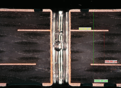
3.2 Via and Plated Through-Hole (PTH) Integrity
- Inspect for voids, cracks, or incomplete plating in vias.
- Ensure barrel cracking is absent (a common failure in thermal cycling).
- Check resin smear in laser-drilled microvias.
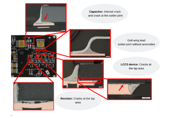
3.3 Solder Joint Quality
- Look for intermetallic compound (IMC) formation (e.g., Cu₆Sn₅ in copper-tin solder joints).
- Detect Kirkendall voids, which weaken solder joints.
- Verify wetting and fillet formation.
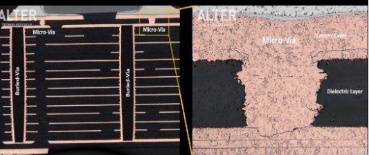
3.4 Delamination and Layer Alignment
- Check for separation between PCB layers (delamination).
- Verify registration accuracy between layers (misalignment can cause short circuits).
3.5 Fiber Weave and Resin Distribution
- Inspect glass fiber distribution in the substrate.
- Detect resin-rich or resin-deficient areas, which affect mechanical strength.
3.6 Surface Finish Examination
- Assess ENIG (Electroless Nickel Immersion Gold), HASL (Hot Air Solder Leveling), or OSP (Organic Solderability Preservative) coatings.
- Look for black pad syndrome (common in ENIG finishes).

4. Common Defects and Their Causes
| Defect | Possible Causes |
|---|---|
| Voids in Plating | Poor electroplating process, trapped air bubbles. |
| Barrel Cracking | Thermal stress, CTE (Coefficient of Thermal Expansion) mismatch. |
| Resin Smear | Excessive heat during drilling, improper desmear process. |
| Delamination | Moisture absorption, poor lamination process. |
| Kirkendall Voids | Uneven diffusion in solder joints, aging effects. |
| Black Pad (ENIG) | Over-etching of nickel, excessive phosphorus content. |
5. Best Practices for Accurate Analysis
- Use multiple microscopy techniques for cross-verification.
- Compare with reference standards (IPC guidelines).
- Document findings with high-resolution images and measurements.
- Avoid over-polishing, which can round edges and obscure defects.
- Control environmental conditions (humidity can affect epoxy curing).
6. Conclusion
PCB microsection analysis is a powerful tool for ensuring reliability in electronics manufacturing. By following proper preparation techniques and using appropriate microscopy methods, engineers can detect hidden defects, improve process controls, and prevent field failures. Regular microsection inspections should be part of a robust quality assurance program in PCB production.