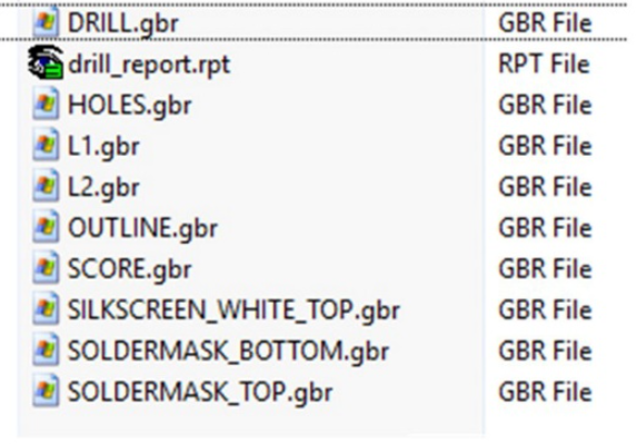
How to design a flex pcb
Understanding how to design a flex pcb
Designing a flexible printed circuit board (flex PCB) requires a comprehensive understanding of both the fundamental principles of PCB design and the unique characteristics that distinguish flex PCBs from their rigid counterparts.
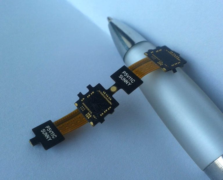
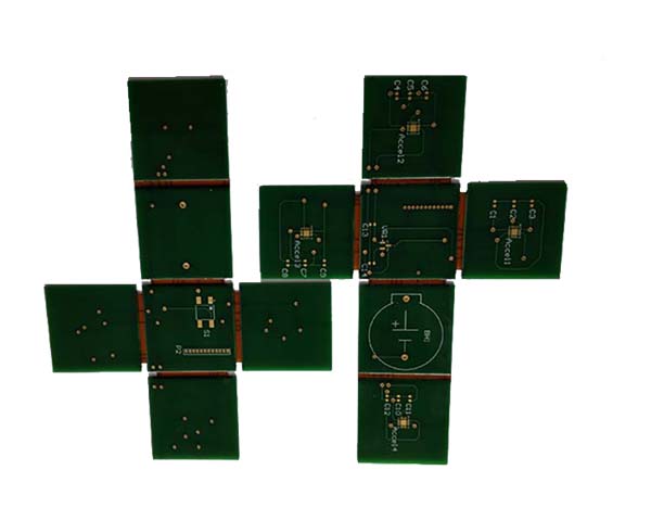
To begin with, it is essential to grasp the basic structure of a flex PCB. Unlike traditional rigid PCBs, flex PCBs are made from flexible materials such as polyimide, which allows them to bend and conform to various shapes. This flexibility makes them ideal for applications where space constraints and mechanical stress are significant considerations.
The first step in designing a flex PCB is to define the requirements and constraints of the project.
This involves understanding the electrical, mechanical, and environmental conditions the PCB will be subjected to. For instance, the designer must consider factors such as the operating temperature range, the amount of flexing the board will endure, and the electrical performance requirements. By clearly defining these parameters, the designer can make informed decisions about material selection, layer stack-up, and trace routing.
Material selection is a critical aspect of flex PCB design.
The choice of substrate material, adhesive, and coverlay can significantly impact the performance and reliability of the final product. Polyimide is a popular choice for the substrate due to its excellent thermal stability and mechanical properties. However, other materials such as polyester may be used for specific applications where cost or other factors are a priority. The adhesive used to bond the layers together must also be carefully selected to ensure it can withstand the mechanical stresses and environmental conditions the PCB will encounter.
Once the materials have been selected, the next step is to design the layer stack-up.
This involves determining the number of conductive layers, the placement of ground and power planes, and the arrangement of signal traces. In flex PCB design, it is crucial to minimize the number of layers to maintain flexibility while ensuring adequate electrical performance. Additionally, the designer must consider the bending radius and the potential for mechanical stress on the traces. To mitigate these issues, it is advisable to use wider traces and avoid sharp corners in the routing.
Trace routing is another critical aspect of flex PCB design.
The designer must ensure that the traces are routed in a manner that minimizes signal interference and maintains signal integrity. This often involves careful planning of the trace layout, including the use of differential pairs for high-speed signals and the placement of decoupling capacitors to reduce noise. Furthermore, the designer must consider the mechanical aspects of the routing, such as avoiding traces that cross over bend areas and ensuring that traces are evenly distributed to prevent stress concentration.
In addition to electrical and mechanical considerations, the designer must also account for manufacturability.
This includes ensuring that the design adheres to the fabrication capabilities of the chosen manufacturer, such as minimum trace width and spacing, hole sizes, and layer alignment tolerances. It is also essential to include appropriate design features such as stiffeners and strain reliefs to enhance the durability and reliability of the flex PCB.
In conclusion, designing a flex PCB requires a thorough understanding of both the electrical and mechanical aspects of PCB design, as well as the unique challenges posed by flexible materials. By carefully defining the project requirements, selecting appropriate materials, designing an optimal layer stack-up, and meticulously routing the traces, the designer can create a flex PCB that meets the desired performance and reliability criteria. Through a methodical and informed approach, the complexities of flex PCB design can be effectively managed, resulting in a successful and robust final product.
Key Materials And Components For Flex PCBs
Designing a flexible printed circuit board (flex PCB) requires a comprehensive understanding of the key materials and components involved. Flex PCBs are known for their ability to bend and twist, making them ideal for applications where space constraints and mechanical flexibility are paramount. To achieve optimal performance, it is essential to select the appropriate materials and components that can withstand the unique demands of flex PCB applications.
One of the primary materials used in the construction of flex PCBs is the substrate.
Polyimide is the most commonly used substrate material due to its excellent thermal stability, mechanical strength, and flexibility. Polyimide substrates can endure high temperatures and harsh environmental conditions, making them suitable for a wide range of applications, from consumer electronics to aerospace. Additionally, polyimide’s low dielectric constant and high dielectric strength contribute to the overall electrical performance of the flex PCB.
Another critical material in flex PCB design is the conductive layer, typically made of copper.
Copper is chosen for its superior electrical conductivity and ductility, which allows it to maintain electrical integrity even when the PCB is bent or flexed. The copper layer is usually deposited onto the polyimide substrate through a process called electroplating or lamination. The thickness of the copper layer can vary depending on the specific requirements of the application, with common thicknesses ranging from 12 to 35 micrometers.
To protect the conductive traces and ensure the longevity of the flex PCB, a coverlay or covercoat is applied
The coverlay, often made of polyimide or a similar flexible material, serves as an insulating layer that shields the copper traces from environmental factors such as moisture, dust, and mechanical abrasion. The coverlay is typically bonded to the substrate using an adhesive, which must be carefully selected to ensure compatibility with both the substrate and the coverlay material. The adhesive should also possess excellent thermal and mechanical properties to maintain the integrity of the flex PCB under various operating conditions.
In addition to the substrate, conductive layer, and coverlay, other components such as stiffeners, connectors, and adhesives play a crucial role in the overall design of a flex PCB.
Stiffeners are rigid materials, often made of FR4 or stainless steel, that are added to specific areas of the flex PCB to provide additional mechanical support and stability. These are particularly useful in regions where components are mounted or where the flex PCB interfaces with other rigid PCBs.
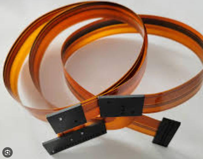
Connectors are another vital component, enabling the flex PCB to interface with other electronic devices or systems.
The choice of connectors depends on factors such as the number of connections required, the mechanical stress the connectors will endure, and the overall design constraints of the application. Common types of connectors used in flex PCBs include ZIF (Zero Insertion Force) connectors, FFC (Flat Flexible Cable) connectors, and board-to-board connectors.
Lastly, adhesives are used not only to bond the various layers of the flex PCB but also to attach components and stiffeners. The selection of adhesives is critical, as they must provide strong adhesion while maintaining flexibility and thermal stability. Epoxy and acrylic-based adhesives are commonly used due to their excellent bonding properties and resistance to environmental factors.
In conclusion, designing a flex PCB involves careful consideration of various materials and components to ensure optimal performance and reliability. By selecting the appropriate substrate, conductive layer, coverlay, stiffeners, connectors, and adhesives, designers can create flex PCBs that meet the specific demands of their applications while maintaining the necessary flexibility and durability.
Best Practices For Flex PCB Layout And Routing
Designing a flexible printed circuit board (flex PCB) requires meticulous attention to detail and adherence to best practices to ensure optimal performance and reliability. The unique properties of flex PCBs, such as their ability to bend and twist, necessitate specific considerations that differ from those of rigid PCBs. To begin with, understanding the material properties is crucial. Flex PCBs are typically made from polyimide, which offers excellent flexibility and thermal stability. This material choice impacts the layout and routing decisions, as it can withstand the mechanical stresses associated with bending.
One of the primary considerations in flex PCB design is the bend radius.
It is essential to maintain an appropriate bend radius to prevent damage to the circuit. A general rule of thumb is to keep the bend radius at least ten times the thickness of the flex PCB. This precaution helps to avoid stress fractures and ensures the longevity of the board. Additionally, it is advisable to use curved traces instead of sharp angles. Sharp angles can act as stress concentrators, leading to potential failure points. By using smooth, curved traces, the stress is distributed more evenly, enhancing the durability of the flex PCB.
Another critical aspect is the placement of components.
When designing a flex PCB, it is important to avoid placing components in areas that will experience significant bending. Components should be located in flat, stable regions to minimize mechanical stress. Furthermore, it is beneficial to use surface-mount technology (SMT) components rather than through-hole components. SMT components are generally smaller and lighter, reducing the overall stress on the flex PCB during bending.
The routing of traces also demands careful consideration.
It is recommended to route traces perpendicular to the bend lines rather than parallel. This orientation helps to distribute the mechanical stress more evenly across the traces, reducing the likelihood of trace breakage. Additionally, maintaining consistent trace widths and spacing is vital. Variations in trace width can create weak points that are susceptible to damage. By keeping the trace widths uniform, the mechanical integrity of the flex PCB is preserved.
Moreover, the use of teardrop pads can enhance the reliability of the flex PCB.
Teardrop pads are designed with a gradual transition from the trace to the pad, reducing the stress concentration at the junction. This design feature helps to prevent pad lifting and trace breakage, especially in areas subjected to repeated bending. In conjunction with teardrop pads, it is also advisable to use filleted corners for pads and vias. Filleted corners distribute stress more evenly, further enhancing the durability of the flex PCB.
Thermal management is another crucial factor in flex PCB design.
The thermal properties of polyimide allow for efficient heat dissipation, but it is still important to consider the thermal load of the components. Proper thermal management can be achieved by incorporating thermal vias and heat sinks, ensuring that the flex PCB operates within safe temperature limits.
In conclusion, designing a flex PCB requires a comprehensive understanding of the material properties and mechanical stresses involved. By adhering to best practices such as maintaining appropriate bend radii, using curved traces, strategically placing components, and ensuring consistent trace widths, designers can create reliable and durable flex PCBs. Additionally, incorporating teardrop pads, filleted corners, and effective thermal management further enhances the performance and longevity of the flex PCB. Through meticulous design and careful consideration of these factors, the unique advantages of flex PCBs can be fully realized.
Common Challenges And Solutions In Flex PCB Design
Designing a flexible printed circuit board (flex PCB) presents a unique set of challenges that differ significantly from those encountered in traditional rigid PCB design. One of the primary challenges is managing the mechanical stress that flex PCBs endure. Unlike rigid PCBs, flex PCBs are designed to bend and twist, which can lead to mechanical fatigue over time. To mitigate this, designers often use materials such as polyimide, which offers excellent flexibility and thermal stability. Additionally, incorporating strain relief features, such as curved traces and filleted corners, can help distribute mechanical stress more evenly across the board.
Another common challenge in flex PCB design is ensuring signal integrity.
The flexible nature of these boards can introduce issues such as signal attenuation and electromagnetic interference (EMI). To address these concerns, designers can employ techniques such as controlled impedance routing and the use of ground planes. Controlled impedance routing helps maintain consistent signal quality by managing the electrical characteristics of the traces, while ground planes can act as shields to minimize EMI. Furthermore, careful consideration of trace width and spacing is crucial to prevent crosstalk and other signal integrity issues.
Thermal management is also a significant concern in flex PCB design.
The materials used in flex PCBs, while excellent for flexibility, often have lower thermal conductivity compared to those used in rigid PCBs. This can lead to hotspots and potential thermal failure if not properly managed. To combat this, designers can use thermal vias and heat sinks to dissipate heat more effectively. Additionally, selecting components with lower power consumption can help reduce the overall thermal load on the board.
Component placement and routing present another set of challenges.
The limited space and the need for flexibility often require creative solutions for placing components and routing traces. One effective strategy is to use a multi-layer design, which allows for more complex routing and better utilization of available space. However, this approach can increase manufacturing complexity and cost. Therefore, a careful balance must be struck between design complexity and manufacturability.
Manufacturing tolerances and material variations can also pose challenges in flex PCB design.
The flexible materials used can have variations in thickness and other properties, which can affect the final performance of the board. To address this, designers should work closely with manufacturers to understand the material specifications and tolerances. This collaboration can help ensure that the design is robust enough to accommodate these variations without compromising performance.
Finally, cost considerations are always a factor in flex PCB design.
The specialized materials and manufacturing processes required for flex PCBs can be more expensive than those for rigid PCBs. To manage costs, designers can optimize the layout to minimize material waste and reduce the number of layers. Additionally, selecting standard components and materials whenever possible can help keep costs down.
In conclusion, while designing a flex PCB comes with its own set of challenges, there are numerous strategies and techniques available to address these issues effectively. By carefully considering mechanical stress, signal integrity, thermal management, component placement, manufacturing tolerances, and cost, designers can create robust and reliable flex PCBs that meet the demands of modern electronic applications. Through a combination of thoughtful design and close collaboration with manufacturers, the complexities of flex PCB design can be successfully navigated.