How to Design a PCB Power Supply System: A Comprehensive Guide
Introduction
Printed Circuit Board (PCB) power supply system design is a critical aspect of electronic product development that directly impacts the reliability, efficiency, and performance of the entire system. A well-designed power supply ensures stable voltage delivery to all components while minimizing noise, heat generation, and electromagnetic interference (EMI). This 2000-word guide will walk you through the essential steps and considerations for implementing an effective PCB power supply system design.
1. Understanding Power Requirements
1.1 Analyzing System Power Needs
The foundation of any power supply design begins with a thorough analysis of your system’s requirements:
- Voltage levels: Identify all required voltages (e.g., 3.3V, 5V, ±12V)
- Current demands: Calculate maximum current for each voltage rail
- Power sequencing: Determine if certain voltages need to come up in a specific order
- Transient response: Consider how quickly the supply must respond to load changes
1.2 Creating a Power Budget
Develop a detailed spreadsheet that lists:
- All active components and their power requirements
- Worst-case and typical consumption scenarios
- Margin considerations (typically 20-30% headroom)
2. Selecting the Power Architecture
2.1 Linear vs. Switching Regulators
Linear Regulators:
- Simple implementation
- Low noise output
- Poor efficiency (especially with large voltage differentials)
- Best for low-power, noise-sensitive applications
Switching Regulators:
- High efficiency (typically 80-95%)
- Can step-up, step-down, or invert voltages
- Generate more noise
- More complex design requirements
2.2 Power Topology Options
- Buck Converters: Step-down voltage
- Boost Converters: Step-up voltage
- Buck-Boost Converters: Handle input voltages above and below output
- LDOs: Low-dropout linear regulators for clean power
- Flyback Converters: Isolated power supplies
2.3 Single vs. Multi-rail Approaches
Consider whether to:
- Use separate regulators for each voltage rail
- Implement a distributed power architecture
- Cascade regulators (e.g., 12V→5V→3.3V)
3. Component Selection
3.1 Voltage Regulators
Key parameters to evaluate:
- Input voltage range
- Output voltage accuracy
- Maximum output current
- Efficiency at your operating point
- Thermal characteristics
- Package size and thermal pad requirements
3.2 Passive Components
Capacitors:
- Ceramic: Low ESR, high frequency response
- Electrolytic: High capacitance, bulk storage
- Tantalum: Good compromise but more expensive
Inductors (for switchers):
- Current rating (watch for saturation)
- DC resistance (affects efficiency)
- Self-resonant frequency
Resistors:
- Precision for feedback networks
- Power rating for current sense applications
4. PCB Layout Considerations
4.1 Power Plane Design
- Dedicate entire layers to power and ground when possible
- Use star topologies to prevent ground loops
- Implement proper plane splitting for multiple voltages
- Consider copper weight (thickness) for high-current paths
4.2 High Current Traces
- Calculate required trace widths using IPC-2152 standards
- Use teardrops at trace junctions
- Implement solder mask defined pads for better current handling
- Consider adding exposed copper with solder for additional current capacity
4.3 Switching Regulator Layout
Critical guidelines:
- Keep high-frequency switching loops small
- Place input capacitors close to regulator pins
- Route feedback paths away from noisy areas
- Use ground planes as shields between noisy and sensitive circuits
4.4 Thermal Management
- Use thermal vias under hot components
- Provide adequate copper area for heat dissipation
- Consider the thermal path to any enclosures or heatsinks
- Place temperature-sensitive components away from heat sources
5. Noise Reduction Techniques
5.1 Filtering Strategies
- Implement π-filters for sensitive analog supplies
- Use ferrite beads where appropriate
- Add small-value ceramic capacitors near IC power pins
- Consider common-mode chokes for noisy environments
5.2 Grounding Techniques
- Separate analog and digital grounds properly
- Use single-point grounding for mixed-signal systems
- Implement ground stitching vias in multilayer boards
- Avoid ground loops that can act as antennas
5.3 EMI Mitigation
- Keep switching nodes small and away from board edges
- Use guard rings around sensitive circuits
- Implement proper shielding where needed
- Consider spread-spectrum techniques for switching regulators
6. Protection Circuits
6.1 Input Protection
- Reverse polarity protection (diodes or MOSFET solutions)
- Overvoltage protection (TVS diodes, clamping circuits)
- Inrush current limiting (NTC thermistors or active circuits)
6.2 Output Protection
- Overcurrent protection (resettable fuses, current limiting circuits)
- Short-circuit protection
- Overvoltage crowbar circuits
- Undervoltage lockout (UVLO) where appropriate
7. Testing and Validation
7.1 Bench Testing
- Verify regulation under various load conditions
- Measure ripple and noise with oscilloscope
- Check transient response to load steps
- Validate thermal performance under worst-case conditions
7.2 Efficiency Measurements
- Calculate efficiency at multiple operating points
- Identify unexpected power losses
- Compare with manufacturer’s specifications
7.3 EMI Testing
- Conduct pre-compliance testing if possible
- Identify problematic frequencies
- Verify effectiveness of filtering and shielding

8. Advanced Considerations
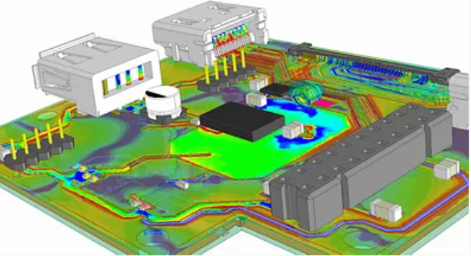
8.1 Power Integrity Analysis
- Perform PDN (Power Distribution Network) impedance analysis
- Use simulation tools to identify potential issues
- Validate with measurements when possible
8.2 Dynamic Voltage Scaling
- Implement adjustable voltage rails for power-sensitive applications
- Consider digital power control (PMBus, AVS)
- Use load switches for power gating unused circuits
8.3 Battery-Powered Considerations
- Implement low-quiescent current designs
- Add fuel gauging and battery management
- Consider energy harvesting options where applicable
Conclusion
Designing an effective PCB power supply system requires careful consideration of numerous factors from initial requirements analysis through final validation. By methodically addressing each aspect—component selection, topology decisions, layout implementation, and protection strategies—you can create power systems that deliver clean, stable power to all components while meeting efficiency, thermal, and reliability targets.
Remember that power supply design is often iterative, with initial prototypes revealing opportunities for optimization. Always build in margin during the design phase to accommodate unexpected loads or operating conditions. With attention to detail and application of these principles, you can develop robust power delivery networks that form the foundation for reliable electronic products.