How to Design Ground (GND) in PCB Layout: Best Practices and Techniques
Introduction to Grounding in PCB Design
Proper grounding is one of the most critical aspects of printed circuit board (PCB) design that directly impacts the performance, reliability, and electromagnetic compatibility (EMC) of electronic devices. The ground (GND) plane serves as the reference point for all signals in the circuit and provides a return path for currents. Poor grounding techniques can lead to issues like ground loops, electromagnetic interference (EMI), signal integrity problems, and even complete circuit failure.
This comprehensive guide explores the fundamental principles and practical techniques for implementing effective ground systems in PCB layouts. We’ll cover different grounding strategies, layer stackup considerations, component placement, and routing techniques that ensure optimal circuit performance.
Understanding Ground Types in PCB Design
Before implementing ground in your PCB layout, it’s essential to understand the different types of ground you may encounter:
1. Analog Ground (AGND)
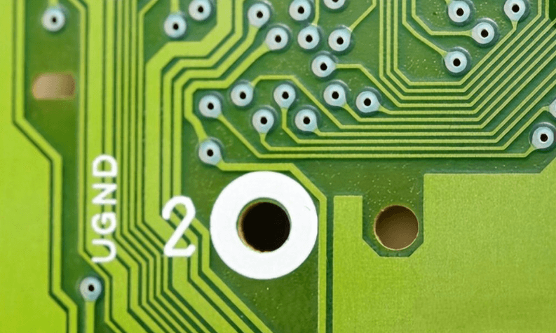
Used for analog circuits where signal integrity is paramount. Analog ground must be kept separate from noisy digital grounds to prevent coupling of digital switching noise into sensitive analog signals.
2. Digital Ground (DGND)
The reference for digital circuits that typically handle high-speed switching signals. Digital grounds can be noisy due to fast current transients.
3. Power Ground (PGND)
Associated with power supply circuits and high-current paths. Often needs special consideration due to high current flows.
4. Chassis Ground
Connects to the metal enclosure or chassis of the device, primarily for safety and shielding purposes.
5. Earth Ground
The actual connection to the earth, typically through the power cord in AC-powered devices.
Fundamental Grounding Strategies
1. Single-Point Grounding
Best for low-frequency circuits (<1MHz) where ground loops are a primary concern. All ground connections meet at a single physical point on the PCB, creating a star topology. This prevents circulating currents between different ground points.
Implementation:
- Identify a central ground point (often near the power supply)
- Route all ground connections radially from this point
- Keep ground traces short and direct
- Avoid creating ground loops
2. Multi-Point Grounding
Preferred for high-frequency circuits (>10MHz) where inductance of ground paths becomes problematic. Creates multiple connections between circuit grounds and the ground plane to minimize ground impedance.
Implementation:
- Use a continuous ground plane
- Make ground connections at multiple points
- Particularly important for high-speed digital circuits
- Helps reduce ground bounce and EMI
3. Hybrid Grounding
Combines single-point and multi-point techniques, often used in mixed-signal designs. Typically employs single-point grounding at low frequencies and multi-point at high frequencies.
Implementation:
- Separate analog and digital grounds
- Connect them at a single point (often under ADCs or DACs)
- Use ferrite beads or 0Ω resistors for isolation when needed
PCB Layer Stackup for Optimal Grounding
The layer stackup of your PCB significantly impacts grounding effectiveness. Here are common configurations:
1. 2-Layer Board Grounding
Challenging but possible with proper planning:
- Dedicate one entire layer as a ground plane when possible
- Use a grid ground structure if a full plane isn’t feasible
- Keep ground traces as wide as possible (minimum 50 mil, preferably wider)
- Use multiple vias to connect ground traces on both layers
2. 4-Layer Board Grounding
The most cost-effective multilayer option with excellent grounding:
- Typical stackup: Signal – Ground – Power – Signal
- The continuous ground plane provides excellent return paths
- Minimizes loop areas and reduces EMI
- Allows controlled impedance routing
3. 6-Layer and Higher Board Grounding
For complex, high-speed designs:
- Multiple ground planes improve signal integrity
- Common stackups include adjacent power and ground planes for decoupling
- Allows stripline routing between ground planes for critical signals
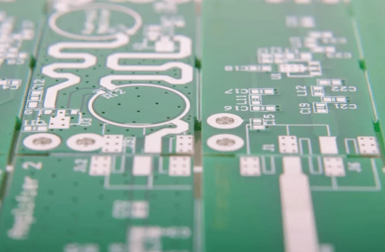
Practical Ground Plane Implementation Techniques
1. Creating a Solid Ground Plane
A solid ground plane is ideal for most applications:
- Fill an entire layer with copper for the ground plane
- Ensure minimal splits or cuts in the plane
- Use thermal relief connections for through-hole components
- Maintain adequate clearance from board edges (typically 20-50 mil)
2. Managing Ground Plane Splits
Sometimes splits are necessary, but must be done carefully:
- Only split planes when absolutely necessary (e.g., isolated circuits)
- Keep splits as narrow as possible
- Route signals over their respective ground regions
- Avoid routing signals over splits (creates impedance discontinuities)
3. Ground Pour in Signal Layers
Even when you have dedicated ground planes, ground pours in signal layers help:
- Improves ground connectivity
- Reduces loop areas for signals
- Helps with heat dissipation
- Connect to main ground plane with multiple vias
Component Placement for Optimal Grounding
1. Power Supply Grounding
The power supply area requires special attention:
- Place bulk capacitors close to power inputs
- Position decoupling capacitors near IC power pins
- Create a solid ground connection under the power supply section
- Use wide traces or polygons for high-current ground paths
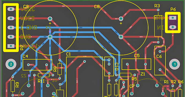
2. Mixed-Signal Grounding
Critical for ADCs, DACs, and sensitive analog circuits:
- Partition the PCB into analog and digital sections
- Maintain separate ground planes if necessary
- Join grounds at a single point under the converter IC
- Route digital signals away from analog sections
3. High-Speed Digital Grounding
For processors, memory, and high-speed interfaces:
- Ensure uninterrupted ground plane beneath high-speed traces
- Place decoupling capacitors very close to IC power pins
- Use multiple vias for ground connections of BGA packages
- Consider via stitching around high-speed connectors
Grounding Specific Circuit Types
1. RF Circuit Grounding
Extremely critical for proper RF performance:
- Use continuous ground planes beneath RF traces
- Implement via fencing around RF transmission lines
- Ensure very low impedance ground connections
- Keep RF grounds separate from digital grounds when possible
2. Motor Control and Power Electronics
Handling high currents and switching noise:
- Use thick copper (2oz or more) for high-current ground paths
- Implement Kelvin connections for current sensing
- Keep high di/dt loops as small as possible
- Consider separate power and signal grounds
3. Sensor Interface Grounding
For sensitive measurements:
- Create a clean, quiet ground region for sensors
- Use star grounding for precision analog circuits
- Shield sensitive traces with guard rings connected to ground
- Implement proper filtering at sensor interfaces
Common Grounding Mistakes to Avoid
- Ground Loops: Creating multiple return paths that can pick up noise.
- Insufficient Ground Connections: Not enough vias connecting ground layers or regions.
- Long Thin Ground Traces: High impedance defeats the purpose of grounding.
- Improper Mixed-Signal Grounding: Allowing digital noise to couple into analog circuits.
- Ignoring Return Current Paths: Not considering where currents actually flow in the ground plane.
- Over-Splitting Ground Planes: Creating unnecessary divisions that cause more problems than they solve.
- Poor High-Frequency Grounding: Not providing low-impedance paths for fast transients.
Advanced Grounding Techniques
1. Via Stitching
Placing multiple vias along ground traces or around perimeter:
- Reduces ground impedance
- Improves heat dissipation
- Enhances EMI shielding
- Typical spacing: λ/10 or closer for RF applications
2. Guard Traces
Ground traces surrounding sensitive signals:
- Shields against crosstalk
- Particularly useful for high-impedance analog signals
- Connect to ground at multiple points
- Keep narrow (typically 10-20 mil width)
3. Moated Ground Regions
Isolated ground areas for extremely sensitive circuits:
- Creates a “quiet” ground zone
- Connected at only one point to main ground
- Useful for precision measurement circuits
- Can be implemented on inner layers as well
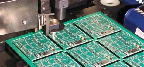
Verification and Testing
After implementing your ground design:
- Visual Inspection: Check for continuity, sufficient via placement, and proper partitioning.
- Continuity Testing: Verify low resistance between all ground points.
- Signal Integrity Analysis: Use simulation tools to check for ground bounce and return paths.
- EMI Testing: Measure radiated emissions to identify grounding issues.
- Function Testing: Verify circuit operation under various load conditions.
Conclusion
Effective ground design in PCBs requires careful planning and execution. By understanding the different grounding strategies, implementing proper layer stackups, and following best practices for component placement and routing, you can create PCB layouts with optimal grounding that ensure reliable operation and meet EMC requirements. Remember that grounding is system-dependent—what works for one design may not be ideal for another. Always consider the specific requirements of your circuit, including signal frequencies, current levels, and noise sensitivity, when implementing your ground scheme.
The key principles to remember are:
- Provide low-impedance return paths for all currents
- Minimize ground loops
- Keep analog and digital grounds separate when necessary
- Understand where currents actually flow in your ground system
- Verify your design through testing and measurement
By applying these grounding techniques, you’ll significantly improve the performance and reliability of your PCB designs.