How to Improve Placement Quality and Efficiency in PCB Prototype Manufacturing
Introduction
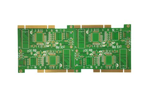
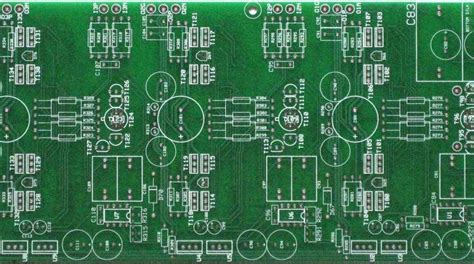
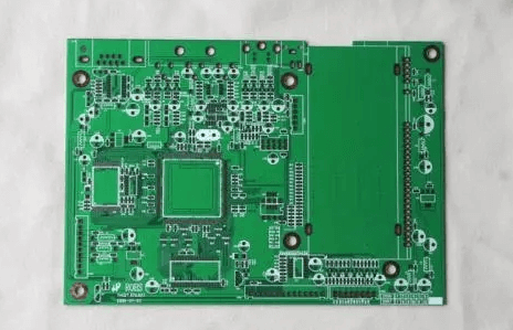
Printed Circuit Board (PCB) prototype manufacturing is a critical phase in electronics development, where design concepts transform into physical boards for testing and validation. The placement process—where surface mount devices (SMDs) and through-hole components are accurately positioned on the PCB—plays a pivotal role in determining the overall quality, functionality, and time-to-market of electronic products. This article explores comprehensive strategies to enhance both placement quality and efficiency in PCB prototype manufacturing.
Understanding Placement Challenges in PCB Prototyping
Before addressing improvement strategies, it’s essential to recognize the unique challenges of PCB prototype manufacturing:
- Small Batch Sizes: Prototypes typically involve small production runs (often single units to a few dozen), making it difficult to achieve economies of scale.
- Frequent Design Changes: Prototypes often undergo multiple iterations with component substitutions and layout modifications.
- Component Diversity: Prototype boards may include a wide variety of component packages, from standard resistors to advanced BGAs and QFNs.
- Time Pressure: Rapid turnaround is often required to maintain development schedules.
- Quality Requirements: Despite being prototypes, these boards must function correctly to provide valid test results.
These factors combine to create a manufacturing environment where both quality and efficiency are challenging yet critical to maintain.
Optimizing Design for Manufacturability (DFM)
1. Implement Comprehensive DFM Guidelines
Design for Manufacturability is the foundation for good placement outcomes:
- Component Selection: Choose components with standardized packaging that is compatible with your placement equipment. Avoid obsolete or hard-to-source parts.
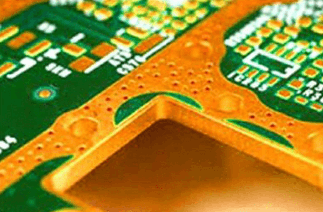
- Footprint Accuracy: Ensure CAD footprints match physical components precisely. Include proper solder mask definitions and pad geometries.
- Component Spacing: Maintain adequate clearance between components (typically ≥0.3mm) to prevent placement interference and enable rework.
- Orientation Consistency: Align similar components in the same direction when possible to minimize pick-and-place head rotations.
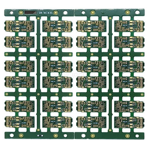
- Panelization: For multiple prototypes, consider panelization with proper breakaway tabs to improve handling efficiency.
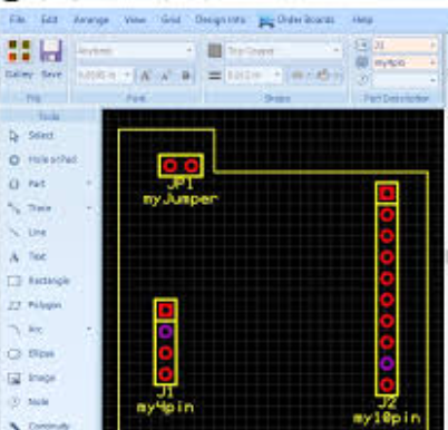
2. Leverage Advanced CAD Tools
Modern PCB design software offers features that directly enhance placement quality:
- Automated DFM Checking: Tools like Valor NPI or CAD-integrated DFM checkers can identify potential placement issues before manufacturing.
- Component Rotation Optimization: Software can analyze and minimize the number of rotation steps required during placement.
- Feeder Configuration Simulation: Some tools can optimize component reel arrangement to reduce pick-and-place machine head movement.
Enhancing SMT Placement Processes
3. Invest in Appropriate Placement Equipment
Selecting the right equipment for your prototype needs is crucial:
- Flexible Pick-and-Place Machines: For diverse prototypes, choose machines with:
- Vision systems capable of handling various component packages
- Quick-change nozzle systems
- Multiple feeder banks
- High placement accuracy (typically ≤50µm)
- Micro-Positioning Capability: Essential for fine-pitch components (≤0.5mm pitch).
- Dual-Lane Systems: Allow simultaneous processing of different board designs.
4. Optimize Machine Programming
Efficient machine programming significantly impacts placement quality and speed:
- Optimal Placement Order: Sequence component placement to minimize head travel distance and rotations.
- Nozzle Selection Strategy: Assign appropriate nozzles for each component type to ensure secure pickup and accurate placement.
- Vision System Calibration: Regularly calibrate fiducial recognition and component inspection systems.
- Dynamic Z-Axis Control: Adjust placement pressure based on component thickness to prevent damage.
5. Implement Advanced Process Controls
- 3D Solder Paste Inspection (SPI): Verify paste volume and alignment before component placement.
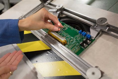
- Automated Optical Inspection (AOI): Post-placement inspection catches errors like misalignment, missing, or wrong components.
- Closed-Loop Feedback: Use inspection data to automatically adjust placement parameters.
Improving Through-Hole Technology (THT) Placement
While SMT dominates modern PCBs, THT components still appear in many prototypes:
6. Selective Use of Automated THT Insertion
For prototypes with multiple THT components:
- Automated Insertion Machines: Can handle axial and radial components with proper programming.
- Pin Straightening: Implement pre-insertion pin conditioning for bent leads.
7. Manual Insertion Best Practices
For low-volume prototypes:
- Custom Insertion Guides: 3D-printed jigs can ensure proper component orientation and positioning.
- Ergonomic Workstations: Proper lighting and magnification reduce insertion errors.
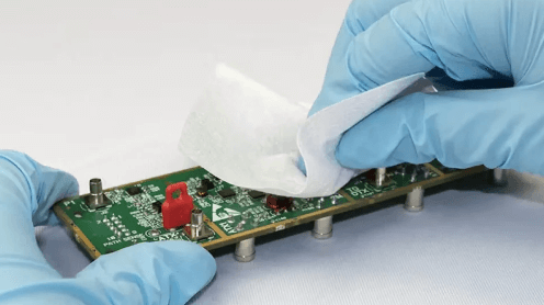
Material and Handling Improvements
8. Optimize Component Packaging and Handling
- Tape-and-Reel Standardization: Where possible, use standardized packaging compatible with auto-feeders.
- Moisture-Sensitive Component Management: Properly store and bake MSD components as needed.
- Component Kitting: For multiple prototypes, pre-organize components by board version.
9. Solder Paste Management
- Paste Selection: Choose appropriate alloy and particle size for your component mix.
- Stencil Design: Optimize aperture geometry and size for each pad.
- Paste Application Control: Maintain consistent printing parameters (speed, pressure, separation).
Workforce and Organizational Strategies
10. Specialized Training Programs
- Machine Operator Certification: Ensure staff are fully trained on placement equipment capabilities.
- Cross-Training: Enable flexibility in staffing assignments.
- Troubleshooting Skills: Teach rapid diagnosis and correction of placement issues.
11. Lean Manufacturing Principles
- Setup Reduction (SMED): Streamline changeovers between different prototype designs.
- Visual Management: Use kanban systems for component replenishment.
- Standard Work Documentation: Create detailed procedures for prototype builds.
Quality Assurance Enhancements
12. Statistical Process Control (SPC)
- Key Metrics Tracking: Monitor first-pass yield, placement accuracy, and defect rates.
- Trend Analysis: Identify recurring issues for systematic correction.
13. Root Cause Analysis
Implement structured problem-solving for placement defects:
- 5 Whys Analysis: Drill down to fundamental causes.
- Fishbone Diagrams: Visualize potential contributing factors.
Emerging Technologies for Placement Improvement
14. Adopt Industry 4.0 Technologies
- Digital Twins: Simulate placement processes before physical production.
- IoT-Enabled Equipment: Real-time monitoring of machine performance.
- Predictive Maintenance: Anticipate and prevent equipment issues.
15. Artificial Intelligence Applications
- Machine Learning for Defect Detection: AI-powered vision systems can identify subtle placement issues.
- Process Optimization Algorithms: AI can suggest optimal placement sequences and parameters.
Continuous Improvement Culture
16. Structured Improvement Programs
- Kaizen Events: Focused workshops to address specific placement challenges.
- Gemba Walks: Regular observation of placement operations to identify improvement opportunities.
17. Knowledge Management
- Lessons Learned Database: Document placement issues and solutions for future reference.
- Best Practice Sharing: Regular team discussions of effective techniques.
Conclusion
Improving placement quality and efficiency in PCB prototype manufacturing requires a holistic approach that addresses equipment, processes, materials, and human factors. By implementing comprehensive DFM practices, optimizing placement equipment and programming, enhancing quality controls, and fostering a culture of continuous improvement, manufacturers can achieve both high-quality prototypes and efficient turnaround times.
The strategies outlined in this article provide a roadmap for PCB prototype manufacturers to:
- Reduce placement defects and rework
- Increase throughput without compromising quality
- Accommodate the unique challenges of prototype production
- Leverage emerging technologies for competitive advantage
As electronic devices continue to increase in complexity while development cycles shrink, excellence in PCB prototype placement becomes ever more critical. Manufacturers who systematically implement these improvement strategies will position themselves as valuable partners in the electronics innovation ecosystem.