How to improve the wiring efficiency in PCB design
The wiring is an extremely important part of the PCB design and it will directly affect the performance of the PCB board. In the PCB design process, layout engineers all have their own understanding of the layout, but all layout engineers are consistent in how to improve the efficiency of wiring, so that not only can save the project development cycle for the customer, but also can ensure the maximum Quality and cost. The following is a general design process and steps.
1, determine the number of PCB layers
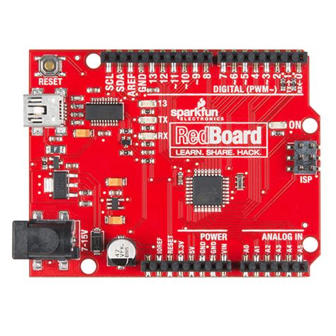
The board size and the number of wiring layers need to be determined early in the design. If the design requires the use of high density ball grid array (BGA) components, the minimum number of wiring layers required to route these devices must be considered. The number of wiring layers and the stack-up method directly affect the wiring and impedance of the printed lines. The size of the board helps to determine the stacking method and the width of the printed lines to achieve the desired design effect.
2, design rules and restrictions
The automatic routing tool itself does not know what to do. To complete the wiring tasks, the wiring tools need to work under the correct rules and restrictions. Different signal lines have different wiring requirements. All special signal lines must be classified. Different design categories are different. Each signal class should have priority. The higher the priority, the stricter the rules. The rules relate to the width of the trace, the maximum number of vias, the parallelism, the mutual influence between the signal lines, and the restrictions of the layers. These rules have a great influence on the performance of the routing tool. Serious consideration of design requirements is an important step in successful cabling.
3, the layout of the components
In order to optimize the assembly process, the Design for Manufacturing (DFM) rules impose restrictions on the layout of components. If the assembly department allows components to move, the circuit can be properly optimized for easier autowiring. The defined rules and constraints affect the layout design.
Zhongguancun Yuankunzhi Workshop is committed to provide one-stop electronic components online procurement services, provide thousands of electronic components procurement, price inquiry and trading, to ensure that all components are from the original channel of the original factory or agent Procurement, guaranteed original authentic, is a professional electronic components procurement site in China
4 fan out design
During the fan-out design stage, the auto-wiring tool must be able to connect the component pins. Each surface-mount device pin should have at least one via hole so that the circuit board can make inner layers when more connections are needed. Connection, in-circuit test (ICT) and circuit reprocessing.
In order to maximize the efficiency of the auto-wiring tool, it is imperative to use the largest via size and traces as much as possible, with an interval setting of 50 mils ideal. Use the type of via that maximizes the number of routing paths. When conducting the fan-out design, consider online circuit test issues. Test fixtures can be expensive and are usually ordered just before full production. It is too late to consider adding nodes to achieve 100% testability.
5, manual wiring and key signal processing
Although this article mainly discusses the issue of auto-wiring, manual cabling is an important process for PCB design now and in the future. Using manual routing helps the automatic routing tool to complete the wiring work. Regardless of the number of critical signals, these signals are first routed, manually routed or combined with automated routing tools. The critical signal must usually pass the careful circuit design to achieve the desired performance. After the wiring is completed, the relevant engineering personnel will check these signal wirings. This process is relatively easy. After the inspection passes, the wires are fixed and then the other signals are automatically routed.
6, automatic routing
The wiring of key signals needs to consider the control of some electrical parameters during wiring, such as reducing the distributed inductance and EMC, and the wiring of other signals is similar. All EDA vendors provide a way to control these parameters. After understanding the input parameters of the automatic routing tool and the influence of the input parameters on the wiring, the quality of the automatic wiring can be guaranteed to some extent.
7, the appearance of the circuit board
Previous designs often paid attention to the board’s visual effects and are now different. The circuit board designed automatically is not more beautiful than the manual design, but it can meet the requirements of the electronic characteristics, and the complete performance of the design is guaranteed.
For layout engineers, whether the technology is severe or not should not be judged only by the number of layers and speed. Only when the number of devices and signal speed are equal, the smaller the area, the lower the number of layers, the lower the cost. The PCB board has been designed to ensure good performance and aesthetics. This is the master.
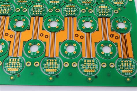
PCB double board wiring principles
PCB board is an important electronic component, and it is the mother body of all electronic components. It has become more and more complex since the beginning of last century. From single layer to double layer, four layers, and multiple layers, the design is also difficult. Increasing. Because both sides of the double-layer board have wiring, understanding and mastering its wiring principles is very helpful for our design. Let’s take a look at the wiring principles of the PCB double board.
The PCB double-layer board ground wire is designed to form a grid-like frame, that is, a plurality of parallel ground wires are laid on one side of the printed board, and the other side is a vertical ground wire of the board, and then metallized vias are connected where they intersect. (The via resistance should be small).
Taking into account that each IC chip should be provided with a ground wire nearby, a ground wire is often clothed every 1 to 115 cm. Such a ground wire makes the area of the signal loop smaller, which is advantageous for reducing radiation. The ground network design method should be before the cloth signal line, otherwise it is more difficult to achieve.
Signal line wiring principle:
After determining the reasonable layout of the components, the double-layer board shall be followed by the design of the ground copy board power cord, and then the important line—sensitive line, high-frequency line, and general line—low frequency line. The critical lead is preferably a separate power supply, ground loop, lead and very short, so sometimes a ground wire is placed close to the signal line on the edge of the critical line to allow it to form a minimal working loop.
The principle of wiring on the top and bottom of the four-layer board is the same as that of the double-layer board.
It is also the first key crystal, crystal oscillator circuit, clock circuit, and CPU signal lines, and the principle of minimizing the circulating current area must be observed.
When the IC circuit of the printed circuit board is working, the circulation area is referred to several times in front, and its conception of differential mode radiation is actually its source. Such as the definition of differential mode radiation: the circuit operating current flows in the signal loop. This signal loop generates electromagnetic radiation. Since this current is differential mode, the radiation generated by the signal loop is called differential mode radiation. Field strength calculation formula:
E1=K1•f2•I•A/γ
In the formula: E1—differential mode copying board The printed circuit board’s radiant field strength in the circuit space γ can be seen from the differential mode radiation formula, and its radiation field strength is proportional to the working frequency f2, circulation area A, and operating current I, such as After the operating frequency f is determined, the size of the circulating current area is a key factor that can be directly controlled in our design.
At the same time, the working speed and current of the circulating current only need to satisfy the reliability, and the bigger the better, the narrower the hop along the signal’s jump edge is, and it’s harmonic. The larger the wave component, the wider the electromagnetic radiation. The higher the power, the greater the current (which has been pointed out above), which we do not expect.
The key link, if possible, is surrounded by ground wires. After the wiring of the PCB copying board is completed, all the voids can be covered with the grounding wire, but it must be noted that these covered grounding wires should be short-circuited with the low-resistance conglomerate of the large strata, so that good results can be obtained (Note: There are voids required Should meet the conditions, such as creepage distance, etc.).