How to Maintain PCB Copper Foil Adhesion: A Comprehensive Guide
Introduction
Printed Circuit Board (PCB) manufacturing relies heavily on the strong adhesion between copper foil and the substrate material. Copper foil adhesion is critical for ensuring the reliability, durability, and performance of electronic circuits. Poor adhesion can lead to delamination, broken traces, and ultimately, circuit failure.
Understanding Copper Foil Adhesion
Copper foil adhesion refers to the bond strength between the copper layer and the substrate (typically FR-4, polyimide, or other dielectric materials). This adhesion is measured in pounds per inch (lb/in) or newtons per meter (N/m) and is essential for:
- Maintaining circuit integrity during thermal cycling
- Preventing delamination during assembly processes
- Ensuring long-term reliability in harsh environments
- Withstanding mechanical stresses during manufacturing and use
Factors Affecting Copper Foil Adhesion
1. Substrate Surface Preparation
The foundation of good copper adhesion begins with proper substrate preparation:
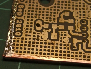
Surface Roughness: Most copper foils used in PCBs are treated with a nodularization process that creates microscopic roughness. The substrate must have appropriate surface characteristics to mechanically interlock with these nodules.
Cleaning: Contaminants like oils, dust, or release agents from manufacturing can significantly reduce adhesion. Isopropyl alcohol (IPA) or specialized cleaning solutions should be used.
Chemical Treatment: Some substrates benefit from chemical treatments that increase surface energy and promote bonding.
2. Copper Foil Type and Treatment
Electrodeposited (ED) Copper: The most common type, featuring a shiny smooth side and a matte rough side. The rough side is treated for better adhesion.
Rolled Annealed (RA) Copper: Has a smoother surface and different crystalline structure, often used in flexible circuits.
Reverse Treat Foil: Features treatment on both sides for multilayer applications.
Low Profile Foils: Designed for high-frequency applications where surface roughness affects signal integrity.
3. Lamination Process Parameters
Proper lamination is crucial for developing strong bonds:
Temperature: Typically ranges from 350°F to 400°F (177°C to 204°C) for FR-4 materials. Temperature must be high enough to flow the resin but not so high as to degrade it.
Pressure: Generally 200-500 psi, ensuring intimate contact without squeezing out all the resin.
Time: Adequate time is needed for the resin to flow and bond with the copper. Typical lamination cycles last 60-120 minutes.
Ramp Rates: Controlled heating and cooling prevent thermal shock that could weaken bonds.
4. Resin System Selection
The substrate’s resin system significantly affects adhesion:
Standard FR-4: Epoxy resin with good general adhesion properties.
High-Tg Materials: May require adjusted lamination parameters.
Polyimide: Excellent thermal properties but may need special surface treatments.
Halogen-Free Materials: Some formulations may have different adhesion characteristics.
Best Practices for Maintaining Copper Adhesion
1. Design Considerations
Copper Weight: Thicker copper (≥2 oz) presents greater challenges for maintaining adhesion.
Trace Geometry: Avoid abrupt width changes that create stress concentration points.
Annular Rings: Ensure adequate size for through-hole components to prevent lifting.
Flex Areas: For rigid-flex designs, consider adhesion requirements in bending regions.
2. Manufacturing Process Control
Storage Conditions: Keep materials in controlled environments (typically 20-25°C, <50% RH).
Handling Procedures: Minimize contact with copper surfaces to prevent contamination.
Process Timing: Minimize time between surface preparation and lamination.
Quality Checks: Implement peel strength testing (IPC-TM-650 2.4.8) at regular intervals.
3. Surface Treatments and Additives
Silane Coupling Agents: Can improve adhesion between inorganic (copper) and organic (resin) materials.
Adhesion Promoters: Special chemical treatments applied before lamination.
Micro-etching: Controlled oxidation can enhance mechanical bonding.
4. Thermal Management
Thermal Cycling Considerations: Design for minimal CTE mismatch between copper and substrate.
Lead-Free Assembly: Higher reflow temperatures require more robust adhesion.
Thermal Relief: Use proper thermal relief patterns for component pads.
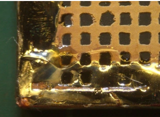
Troubleshooting Poor Adhesion
Common Symptoms:
- Copper lifting during drilling or routing
- Blistering or delamination after soldering
- Measured peel strength below specifications (typically <6 lb/in for 1 oz copper)
Diagnostic Steps:
- Visual Inspection: Examine failure interfaces for contamination or improper bonding.
- Peel Testing: Quantify adhesion strength according to IPC standards.
- Cross-Section Analysis: Examine bond interface under magnification.
- Thermal Analysis: Check for resin degradation or incomplete cure.
Corrective Actions:
- Adjust lamination parameters (temperature, pressure, time)
- Improve surface preparation
- Change copper foil type or treatment
- Modify resin system or additives
Advanced Techniques for Enhanced Adhesion
1. Plasma Treatment
Low-temperature plasma can:
- Clean surfaces at molecular level
- Increase surface energy
- Create functional groups for chemical bonding
2. Laser Surface Preparation
Precise laser treatment can create optimized surface topography without contamination.
3. Nanotechnology Approaches
- Nano-structured copper surfaces
- Nanoparticle-doped resins
- Molecular adhesion promoters
4. Alternative Bonding Methods
- Direct metallization processes
- Adhesive-less laminates for flexible circuits
- Ultrasonic bonding techniques
Industry Standards and Specifications
IPC-4101: Specification for base materials for rigid and multilayer boards.
IPC-TM-650 2.4.8: Test method for peel strength of metallic clad laminates.
IPC-6012: Qualification and performance specification for rigid PCBs.
MIL-P-50884: Military specification for flexible circuits (includes adhesion requirements).
Future Trends in Copper Adhesion Technology
- Ultra-Thin Copper: Developing reliable adhesion for 3µm and thinner foils.
- High-Frequency Materials: Balancing adhesion with surface roughness requirements.
- Sustainable Materials: Maintaining performance with eco-friendly substrates.
- Additive Processes: Adhesion challenges in printed electronics.
Conclusion
Maintaining optimal PCB copper foil adhesion requires attention to multiple factors throughout design, material selection, and manufacturing processes. By understanding the mechanisms of adhesion, implementing proper process controls, and staying informed about new technologies, manufacturers can ensure reliable bonds that withstand the demands of modern electronics. Regular testing and process monitoring are essential for catching adhesion issues before they lead to field failures. As PCB technology continues to evolve with thinner traces, higher densities, and more challenging operating environments, copper adhesion will remain a critical focus area for quality and reliability.
Implementing the practices outlined in this article will help PCB manufacturers and designers:
- Reduce field failures related to delamination
- Improve yields in manufacturing
- Enable more reliable high-density designs
- Extend product lifespan in harsh environments
By making copper foil adhesion a priority throughout the product lifecycle, the electronics industry can continue to push the boundaries of performance while maintaining the reliability that users demand.