How to make some trade-offs when designing PCB boards to make the power distribution of PCBs
When designing more complex boards, you must make some design trade-offs, and these trade-offs will have some factors that affect the design of the power distribution network of the PCB.
When the capacitor is installed on the PCB board, there will be an additional loop inductance, which is related to the installation of the capacitor. The size of the loop inductance value depends on the design, and the size of the loop inductance depends on the line width and line length of the line from the capacitor to the via. The length of the trace is the length of the connecting capacitor and the power/ground plane, the distance between the two holes, the diameter of the hole, the pad of the capacitor, etc. As shown in Figure 1, the installation diagram of various capacitors:
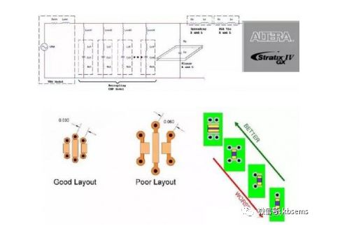
Figure 1 The best and worst capacitor layout
Design points for reducing capacitor loop inductance
■The hole should be placed as close to the capacitor as possible. Reduce the hole spacing of the power/ground. If possible, use multiple pairs of power/ground holes in parallel. For example, place two holes with opposite current polarity as close as possible, and place holes with the same current polarity as far as possible.
■Use short and wide traces to connect the hole and the capacitor pin.
■ Place capacitors on the surface of the PCB (top and bottom layers) as close to their corresponding power/ground planes as possible, which can reduce the distance between holes. Use thin dielectrics between power/ground.
For the mounting and propagation inductance of capacitors, the following are three different designs. Figure 2 shows how various design situations introduce loop inductance:
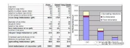
Figure 2 Best and worst capacitor layout
Case 1 – Poor design
■ The designer does not pay attention to the design of the power distribution network (PDN).
■ The spacing of the holes is not optimized.
■ The distance between the power and ground planes is not optimized.
■ The trace distance from the hole to the capacitor pin is long.
For the total loop inductance, the loop inductance mainly comes from the routing, because the line length of the poor design is 5 times longer than that of the other two cases (better design and very good design). The distance from the bottom layer where the capacitor is mounted to the nearest plane is also a major factor in the loop inductance, because this is not optimized (10mil), the routing has a great impact on the total loop inductance. Again, because the designer used 10 mils of dielectric material between power and ground, the secondary contributor to loop inductance is propagation inductance. The effect of not optimizing the distance between vias is less significant than the length of the vias, and the effect of the vias becomes greater for longer vias.
Case 2 – Good Design
■ The designer paid some attention to the design of the power distribution network (PDN).
■ The spacing of the vias was improved, and the length of the vias remained the same.
■ The distance between the power and ground planes was improved.
■ The trace distance from the vias to the capacitor pins was optimized.
The trace loop inductance is still the main contributor to the total loop inductance. The trace loop inductance of the good design is about 2.7 times smaller than the trace loop inductance of the poor design case, because the designer reduced the thickness of the dielectric from 10 mils to 5 mils, reducing the propagation inductance by half. The effect of the vias is slightly improved due to the reduction in the distance between the vias.
Case 3 – Very Good Design
■ The designer paid great attention to the design of the PDN.
■The hole spacing and length have been improved.
■The distance between power and ground has been fully optimized.
■The trace distance from the via to the capacitor pin has been optimized.
The inductance of the very well designed trace is about 7.65 times smaller than the inductance of the poorly designed trace. This is achieved by reducing the trace length and reducing the thickness of the bottom surface from the capacitor to the nearest plane layer on the PCB. Since the designer has optimized the thickness of the dielectric layer between the power and ground, the propagation inductance is greatly reduced. The loop inductance of the via has been significantly improved by greatly reducing the hole spacing and hole length. Compared with the poor design, the total loop inductance of the very well designed case is reduced by reducing one of the seven major factors. .
In the PCB board, additional via loop inductance is introduced by mounting the capacitor, which reduces the resonant frequency of the capacitor. This factor must be considered when you are designing the power distribution network (PDN). Reducing the loop inductance is the only visible way to reduce impedance when designing at high frequencies.
For a given power supply, the report generated by the PDN tool shows that the PCB cutoff frequency is higher for the very good design compared to the very good design and the poor design. This may be the opposite of what is expected because more capacitors are required to decouple the higher cutoff frequency than to decouple the lower cutoff frequency.
For the very good design case, the higher cutoff frequency means that the higher frequencies can be decoupled. The capacitors placed on the PCB have a decoupling effect on the noise up to the higher frequencies.
For the poor design case, the PCB cannot be decoupled above the lower cutoff frequency. Any additional capacitance, that is, adding decoupling capacitors above the cutoff frequency, only increases the BOM cost without any effect on the decoupling effect. For this poor design case, the design of the power distribution network is more susceptible to noise at a certain frequency than for the very good design.
As another example, assume that a 20-layer PCB has a total thickness of 115mil. The power layer is on the third layer. The thickness from the first layer (the layer where the FPGA is located) to the third layer is 12mil, so the thickness from the bottom layer to the third layer is 103mil. The power and ground layers are separated by a 3mil dielectric. The inductance of the BGA hole for this track is 5nH (5 pairs of holes for this power track). In order to cope with the relatively dense layout and routing area on the first layer, the associated decoupling capacitors are installed on the bottom layer. Since such installation will have very long vias, this trade-off design leads to a high capacitor installation inductance value. After full optimization, the installation inductance of the 0402 package capacitor on the bottom layer is 2.3nH, while the installation inductance of the same capacitor on the first layer is 0.57nH.
To improve the PDN effect of this track, you can place some high-frequency capacitors on the first layer, while keeping the mid-frequency and bulk capacitors in their original positions, that is, the bottom layer. This circuit design is a cut-off solution for PDN, because the high-frequency capacitor is the first response capacitor below the cut-off frequency. The effect of the capacitor depends on the total loop inductance (mounting inductance of the capacitor + propagation inductance + inductance of the BGA hole) and the FPGA. You can place the high frequency capacitor on the first layer and slightly away from the FPGA. The propagation inductance of the capacitor outside the FPGA breakout area is 0.2nH. Compared with the original method of placing it on the bottom layer, this new placement method is still beneficial because the total loop inductance (0.57nH+0.2nH+0.05nH=0.82nH) is smaller than the total inductance when placed on the bottom layer.
The propagation inductance of the PCB board is design-dependent and exists uniformly in the dielectric between the power and ground planes. 3mil thickness or thinner is the best design to reduce the plane propagation inductance. You can improve the performance of the PDN by following the following design guidelines.
The following are design guidelines on the importance of order, from the first layer to the bottom layer, where the design guidelines on the first layer are the most important.
■ Reduce the dielectric thickness between the power and ground layers. When designing the board stackup, determine the power, layer, and other layers. For example, a stackup of PWR1 – GND1 – SIG1 – SIG2- GND2 – PWR2 is better than a stackup of PWR1 – SIG1 – GND1 – SIG2 – GND2 – PWR2. The second case is the result of a design that does not optimize the distance between power and ground, which results in a large capacitor propagating more inductance between PWR1/GND1 than between PWR2/GND2. You can find a typical dielectric thickness of 3 mils between the power and ground planes without adding extra cost. For additional performance improvement, consider a dielectric thickness thinner than 3 mils, but this will increase the cost of the PCB.
■ When selecting capacitors, select multiple capacitor values instead of selecting a large capacitor of the same value to achieve the target impedance. In a PDN, the peak of the impedance is formed by a resonant reaction. A high ESR at the resonant frequency can suppress the resonance, thereby reducing the height of the impedance peak. Using a few capacitors of the same capacitance value at the capacitor’s resonant frequency and the impedance peak can effectively reduce the ESR.
A wide range of frequencies can be achieved by selecting capacitors with a variety of capacitance values to maintain a relatively high ESR.
■ Choose the location of high-frequency capacitors to reduce the total loop inductance. The total inductance is composed of the capacitor’s ESL, mounting inductance, propagation inductance, and BGA via inductance. When placing capacitors, prioritize high-frequency capacitors, followed by mid-frequency and low-frequency capacitors.
■ When splitting planes, make sure the planes are properly square. Avoid narrow plane shapes, as this will limit the current and increase the plane’s propagation inductance.
■ There is less sensitivity to how to place mid-frequency and low-frequency capacitors, so place them slightly further away from the FPGA.
Weighing the situation of multi-channel design
On a PCB with multiple peripherals, your design can no longer share a single power supply. This may require you to implement DDR power interfaces through your design, combine power traces of various I/O ports, or combine power traces of various receivers to reduce PCB BOM cost and PCB layout complexity.
Power trace sharing increases the complexity of the PDN and also adds a lot of noise at the PCB and die locations. For multiple power supply situations, there are two main steps to designing a power distribution solution:
- Low frequency solution
- High frequency solution
At very low frequencies, the first step is to ensure that the VRM is sized appropriately to handle the various current needs.
Low frequency decoupling must take into account the currents of various power supply combinations. Bulk capacitors must be selected to cover the frequency band covered by the target impedance. It is difficult to know the frequency range accurately because there is an area beyond the impedance curve. This is a given power supply area on the die, based on its own maximum current consumption, rather than the current consumption of other currents associated with the same power supply combination. For the design, the frequency range of bulk capacitor decoupling is estimated to be from DC to about 5~10MHz.
When sharing multiple power supplies, use this design method in a similar way through the PDN tool, but it is recommended that you decouple at the highest cutoff frequency point. For decoupling of single and shared multiple power supplies, this is the process for successfully implementing a single PDN method design. This method is suitable for power supply circuit design with similar current requirements between power supply circuits. However, there are several exceptions to this method.
This example is that the power supply is shared between the core power supply (Vcc) and the PCI Express hard IP Block (VccHIP) power supply. The reasons for the exception are:
■ The current of VCC will be much larger than that of VCCHIP.
■ Compared with VCC and VCCHIP, the via inductance of BGA of VCC will be much lower than that of VCCHIP.
■ Compared with VCC and VCCHIP, the cutoff frequency of VCC will be much lower than that of VCCHIP.
Therefore, for power supply design, it is not applicable to use the highest cutoff frequency decoupling at the BGA via. As shown in Figure 3, the combined impedance curve of VCC and VCCHIP power supply circuits does not meet the target impedance, which is equivalent to not meeting the cutoff frequency decoupling of VCCHIP. This is because the decoupling capacitor effect is limited.
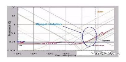
Figure 3 Cutoff frequency impedance curve of VCCHIP
According to the previous explanation, high-frequency noise in the power supply track is mainly generated by its own transient current. The decoupling design guideline for the highest cutoff frequency of the shared circuit is based on the impedance calculation of the entire transient current, which is the requirement of “over-design”.
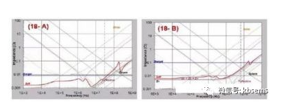
Figure 4 Changing the sharing of the power path
In this case, you must calculate the target impedance curve based on the entire transient current based on the PCB decoupling project, which is equivalent to the maximum current consumption of the power path cutoff frequency. In the example of VCC and VCCHIP power paths shared, you must use the cutoff frequency of the VCC power path. Figure 3 shows the impedance curve of the combined power path at the cutoff frequency of the core power decoupling. For the core power, the impedance curve is obtained by the total current (VCC+VCCHIP) along the balls or vias of the BGA. Then you can check whether the verification result meets the target impedance of the single power design guideline.
Based on the same decoupling project as Figure 4-A, Figure 4-B shows the impedance curve of the VCCHIP power supply. However, when obtaining this curve, only the current consumption and the number of BGA vias need to be considered for VCCHIP. As shown in Figure 4-B, the impedance curve of VCCHIP reaches the target impedance until the cutoff frequency of the VCCHIP power supply.
The final decoupling project must reach the frequency of the respective target impedance. If there are some special violations of the design goals, the decoupling project can be optimized as little as possible.
In similar situations, any power supply combination can be optimized according to the example of VCC and VCCHIP.
On a PCB board, when there are multiple FPGAs that need to be powered from the same power supply, you can use a similar approach to deal with this situation. For designing low-frequency solutions, you must use the total current consumption of the chips. For designing high-frequency solutions, you must use the current consumption of one of the chips. You can use the same number of capacitors to decouple other chips at high frequencies.
When compared with the solution obtained by the field analysis tool, if the space between the two FPGA chips is small, the high-frequency side may result in a slight over-design, because the field analysis tool takes into account the layout of the board. This may be because the chips are close together and there is no capacitor that can meet the requirements of the location of the two chips. This also depends on the capacitor’s cut-off loop inductance seen from the FPGA chip side.
A common design trade-off is to create a separate power plane and power different power networks from one power supply, using filters to provide clean power to the power network. In most cases the filter is a ferrite bead connected between two power supplies on the board. As a rule, you can provide clean power to a power network by following the design guidelines below.
■When the ferrite bead is connected between two power networks, make sure the mounting inductance is minimal.
■Choose the ferrite bead based on the characteristics listed below, making sure the current consumption of the power circuit is less than the rated current of the ferrite bead.
■Package size (0603, 0402, etc.)
■Rated current
■DC resistance
■Impedance at the target frequency (10 MHz, 100 MHz, 1 GHz, etc.)
■The frequency response of the equivalent RLC model of the bead must be as consistent as possible with that given in the datasheet.
■When doing AC analysis, the model of the bead must be included in the covered frequency range, as well as the various capacitors selected to achieve the target impedance. When designing the equivalent RLC model of the capacitor, the mounting inductance must be considered as a component of the model. If the AC analysis does not have a peak in the frequency band of interest (DC to 200 MHz), you can use the bead isolation to provide clean power.
■The PDN results obtained through the above simulation must meet the requirements of the target impedance in the frequency band of interest.


