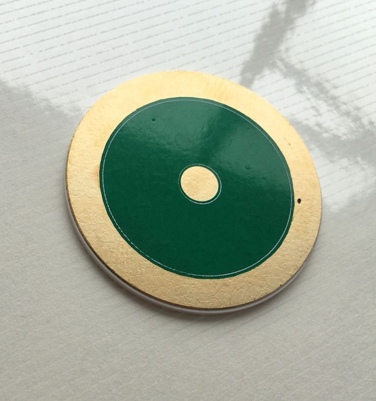
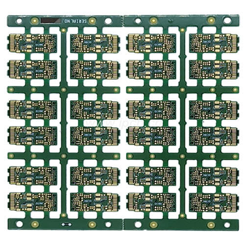
How to use a pcb prototype board
Step-by-Step Guide to Soldering Components on a PCB Prototype Board
Soldering components onto a PCB prototype board is a fundamental skill for anyone involved in electronics. This process, while intricate, can be mastered with careful attention to detail and adherence to proper techniques. To begin, gather all necessary tools and materials, including the PCB prototype board, soldering iron, solder, flux, tweezers, and the electronic components you intend to use. Ensuring that you have a clean, well-lit workspace is also crucial for precision and safety.
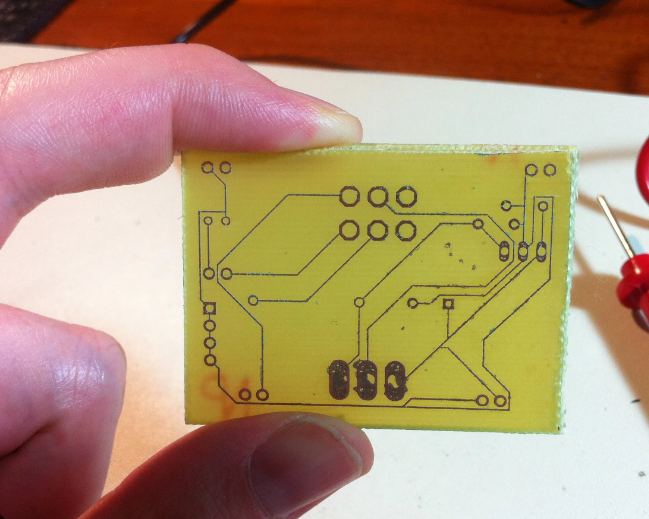
Start by preparing the PCB prototype board.
Inspect the board for any visible defects or contaminants that could interfere with the soldering process. If necessary, clean the board using isopropyl alcohol and a lint-free cloth to remove any oils or residues. This step is essential as it ensures that the solder will adhere properly to the board.
Next, organize your components.
Lay them out in the order they will be soldered onto the board. This organization helps streamline the process and reduces the risk of errors. Refer to the schematic diagram of your circuit to ensure that each component is placed in the correct position. Double-check the orientation of polarized components, such as diodes and electrolytic capacitors, as incorrect placement can lead to circuit malfunction.
Once your components are organized, begin the soldering process by pre-tinning the soldering iron tip.
Heat the iron to the appropriate temperature, typically around 350°C (662°F), and apply a small amount of solder to the tip. This step improves heat transfer and facilitates smoother soldering.
Proceed by applying a small amount of flux to the pads on the PCB where the components will be placed.
Flux helps clean the metal surfaces and enhances the flow of solder, resulting in stronger, more reliable joints. Using tweezers, carefully position the first component onto the board. Hold the component in place and touch the soldering iron tip to the pad and the component lead simultaneously. Feed solder into the joint, allowing it to flow and form a secure connection. Remove the soldering iron and let the joint cool naturally. Avoid moving the component during this cooling period to prevent a cold joint, which can lead to poor electrical connectivity.
Continue this process for each component, working methodically to ensure accuracy.
For components with multiple leads, such as integrated circuits, it is often helpful to solder one corner lead first to secure the component in place before soldering the remaining leads. This technique minimizes the risk of misalignment.
After all components are soldered, inspect each joint carefully.
A good solder joint should be smooth, shiny, and conical in shape. If any joints appear dull, cracked, or have excess solder, rework them by reheating and applying additional solder as needed. Trim any excess leads using flush cutters to prevent short circuits.
Finally, clean the PCB to remove any residual flux, which can be corrosive over time. Use isopropyl alcohol and a brush to gently scrub the board, ensuring all flux residues are removed. Allow the board to dry completely before testing the circuit.
By following these steps meticulously, you can achieve a well-soldered PCB prototype board that is both functional and reliable. Mastery of this process not only enhances your technical skills but also lays the foundation for successful electronic projects.
Designing Your First Circuit: Tips for Using a PCB Prototype Board
Designing your first circuit using a PCB prototype board can be an exciting yet challenging endeavor. To ensure a smooth process, it is essential to follow a series of well-defined steps and adhere to best practices. Initially, it is crucial to have a clear understanding of your circuit’s requirements and specifications. This involves creating a detailed schematic diagram that outlines the components and their connections. By doing so, you lay the groundwork for a successful design and minimize the risk of errors during the assembly phase.
Once you have a comprehensive schematic, the next step is to select an appropriate PCB prototype board.
These boards come in various sizes and configurations, so it is important to choose one that accommodates your circuit’s complexity and component density. Additionally, consider the board’s material and thickness, as these factors can influence the overall performance and durability of your circuit.
With your PCB prototype board in hand, the next phase involves placing the components onto the board.
It is advisable to start with the larger components, such as integrated circuits and connectors, as these will serve as reference points for the placement of smaller components. To ensure optimal performance, pay close attention to the orientation and alignment of each component. This is particularly important for polarized components, such as capacitors and diodes, which must be placed in the correct direction to function properly.
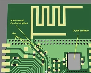
As you place the components, it is essential to consider the layout of the traces that will connect them.
Traces are the conductive pathways that allow electrical signals to flow between components. To minimize signal interference and ensure reliable operation, it is important to keep traces as short and direct as possible. Additionally, avoid placing traces too close to one another, as this can lead to short circuits and other issues. Utilizing a grid system can help maintain an organized and efficient layout.
After placing the components and planning the traces, the next step is to secure the components to the PCB prototype board.
This is typically done using solder, a fusible metal alloy that creates a strong electrical and mechanical bond between the components and the board. When soldering, it is important to use the appropriate type and amount of solder, as well as the correct temperature settings on your soldering iron. Excessive heat or solder can damage components and create unreliable connections.
Once all components are securely soldered in place, it is crucial to inspect the board for any potential issues
This includes checking for cold solder joints, which are weak connections that can cause intermittent failures, as well as ensuring that there are no unintended bridges between traces. Using a magnifying glass or microscope can help identify these issues more easily.
Finally, it is time to test your circuit.
Begin by performing a visual inspection to ensure that all components are correctly placed and soldered. Next, use a multimeter to check for continuity and verify that there are no short circuits. Once you are confident that the circuit is free of defects, power it on and observe its behavior. If the circuit does not function as expected, systematically troubleshoot by checking each component and connection.
In conclusion, designing your first circuit using a PCB prototype board requires careful planning, attention to detail, and methodical execution. By following these tips and best practices, you can increase the likelihood of creating a functional and reliable circuit. As you gain experience, you will develop a deeper understanding of the intricacies involved in PCB design and assembly, ultimately leading to more complex and sophisticated projects.
Common Mistakes to Avoid When Working with PCB Prototype Boards
When working with PCB prototype boards, it is essential to be aware of common mistakes that can hinder the success of your project. One frequent error is neglecting to thoroughly plan the layout before beginning the assembly process. Without a well-thought-out design, you may encounter issues such as overlapping traces or insufficient space for components, which can lead to short circuits or signal interference. To avoid this, it is advisable to use PCB design software to create a detailed schematic and layout, ensuring that all components fit properly and that traces are optimally routed.
Another common mistake is improper soldering techniques.
Poor soldering can result in weak connections, which may cause intermittent faults or complete circuit failure. It is crucial to use the correct type of solder and to ensure that your soldering iron is at the appropriate temperature. Additionally, take care to avoid cold solder joints by allowing the solder to flow smoothly and fully around the component leads and pads. Practicing good soldering habits, such as cleaning the tip of the soldering iron regularly and using flux to promote better adhesion, can significantly improve the reliability of your connections.
Furthermore, overlooking the importance of component placement can lead to functional and thermal issues.
Placing components too close together can cause overheating and make it difficult to troubleshoot or replace parts if necessary. It is important to follow the manufacturer’s guidelines for component spacing and to consider the thermal management of your board. Using heat sinks, thermal vias, and proper ventilation can help dissipate heat and maintain the performance and longevity of your PCB.
In addition to these technical aspects, it is also essential to pay attention to the quality of the materials used.
Using substandard components or PCB materials can compromise the integrity of your prototype. Ensure that you source components from reputable suppliers and verify their specifications to match your design requirements. High-quality materials not only enhance the performance of your PCB but also reduce the likelihood of defects and failures.
Another pitfall to avoid is inadequate testing and debugging.
Skipping or rushing through the testing phase can result in undetected errors that may become costly to fix later. It is important to perform thorough testing at each stage of the assembly process, from individual component testing to full system integration. Utilizing tools such as multimeters, oscilloscopes, and logic analyzers can help identify and resolve issues early on. Additionally, creating a comprehensive test plan and documenting your findings can streamline the debugging process and improve the overall quality of your prototype.
Lastly, failing to consider the manufacturability of your PCB design can lead to complications during mass production.
While a prototype board allows for some flexibility and manual adjustments, transitioning to large-scale production requires a design that is optimized for automated assembly processes. Ensuring that your design adheres to industry standards and guidelines, such as those outlined by the IPC (Institute for Printed Circuits), can facilitate a smoother transition from prototype to production.
In conclusion, avoiding these common mistakes when working with PCB prototype boards can significantly enhance the success of your project. By meticulously planning your layout, employing proper soldering techniques, considering component placement and thermal management, using high-quality materials, conducting thorough testing, and designing for manufacturability, you can create reliable and efficient PCB prototypes that meet your design objectives.
Essential Tools and Materials for PCB Prototype Board Projects
When embarking on a project involving a PCB prototype board, it is crucial to gather the essential tools and materials to ensure a smooth and efficient process. The first step in any PCB prototyping endeavor is to have a clear understanding of the components and equipment required. This preparation not only streamlines the workflow but also minimizes the risk of errors and rework.
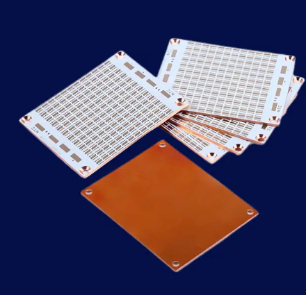
To begin with, a high-quality PCB prototype board is indispensable.
These boards come in various sizes and configurations, so selecting one that suits the specific requirements of your project is paramount. Alongside the board, a reliable soldering iron is essential. A soldering iron with adjustable temperature settings is particularly advantageous, as it allows for precise control over the soldering process, thereby reducing the likelihood of damaging sensitive components.
In addition to the soldering iron, solder wire is another critical material.
Lead-free solder is often recommended due to its environmental benefits and compliance with safety standards. However, it is important to choose solder wire with an appropriate diameter for the components being used. Flux, which aids in the soldering process by preventing oxidation and improving the flow of solder, should also be on hand.
Furthermore, a set of tweezers is invaluable for handling small components with precision.
Tweezers with fine tips are particularly useful for placing and adjusting components on the PCB prototype board. To complement the tweezers, a magnifying glass or a microscope can be extremely helpful, especially when working with miniature components or intricate circuit designs.
Another essential tool is a multimeter, which is used to measure voltage, current, and resistance.
This device is crucial for testing and troubleshooting the circuit to ensure that it functions as intended. Additionally, a set of wire cutters and strippers is necessary for preparing and managing the wiring involved in the project.
To organize and secure components during the assembly process, a breadboard can be used. This tool allows for temporary construction and testing of circuits before finalizing the design on the PCB prototype board. It is also beneficial to have a set of jumper wires for making connections on the breadboard.
Moreover, a power supply is required to provide the necessary voltage and current to the circuit.
Adjustable power supplies are particularly useful as they offer flexibility in testing different voltage levels. Alongside the power supply, having a set of alligator clips can facilitate easy and secure connections to the circuit.
For those who prefer a more automated approach, a soldering station with a built-in fume extractor can be a worthwhile investment. This setup not only provides a stable platform for soldering but also ensures a safer working environment by removing harmful fumes generated during the soldering process.
Lastly, it is important to have a well-organized workspace. A clean and clutter-free environment reduces the risk of losing small components and allows for more efficient workflow. Storage containers and labeling systems can help keep components and tools organized and easily accessible.
In conclusion, assembling the essential tools and materials for PCB prototype board projects is a foundational step that significantly impacts the success and efficiency of the endeavor. By ensuring that you have high-quality equipment and a well-organized workspace, you can focus on the intricate task of designing and assembling your circuit with confidence and precision.