Humidity:A Major Factor Affecting PCB Assembly
This article clearly identifies humidity-related issues in printed circuit board.It’s a precise article on mitigating the effects of moisture on any type of printed circuit board.From material integration,PCB layout protyping,PCB engineering,assembly,to packing and order delivery,attention should be paid to the effects of moisture in PCB manufacturing to avoid damage and other issues with PCB functionality.Furthermore,let’s delve into the important measures for controlling humidity levels during the lamination process,controls implemented during PCB assembly,and controlled storage packaging,and shipping.
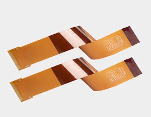
Rigid/flexible printed circuit board assemblies,cable harnesses,boxed assemblies,or wire harness PCB assemblies are made from a variety of materials that perfectly match the properties required for roubust mechanical and electrical performance in electronic products used across all major industries worldwide.Demanding high frequency,low impedance,compactness,durability,high tensile strength,low weight,multifunctionality,temperature control,or humidity resistance,PCBs are available in single,double,or multi-layer configurations,depending high frequency,low impedance ,compactness,durability,high tensile strength,low weight,multifunctionality,temperature control,or humidity resistance,PCBs are available in single,double,or multi-layer configurations,depending on the complexity of the circuitry.of all the serious issues that should be addressed during the initial stages of PCB manufacturing, humidity or moisture is a major factor that creates the potential for electronic and mechanical failures during PCB operation.

How does moisture cause significant trouble in printed circuit boards ?
Moisture can cause various defects in PCB assemblies by accumulating in epoxy-glass prepreg,duffusing within the PCB during storage,and absorbing it.Moisture can accumulate in microcracks or form a home in the resin interface during wet processing during PCB manufacturing.High temperatures and vapor pressures,coupled with the high pressures associated with the quadrilateral structure of PCB assembly,can lead to moisture absorption.
As adhesive and cohesive failures in printed circuit boards lead to delamination or cracking,moisture can enable metal,resulting in low-impedance paths with altered dimensional stability.With technically more detrimental effects such as a lowering of the glass transition temperature and an increase in the dielectric constant,it can lead to reduced circuit switching speeds and increased propagation delays.
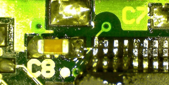
The primary impact of moisture in PCBs is that it degrages the quality of metallization,lamination,solder mask,and the PCB manufacturing process.Due to moisture,thermal stress limits are exceeded as the glass transition temperature decreases.Sometimes, it can also cause severe short circuits, leading to moisture ingress and ionic corrosion. Other common properties of printed circuit board assemblies that are affected by moisture absorption include flame retardancy or delamination, increased dissipation factor (DF) and dielectric constant (DK), thermal stress on plated through holes, and copper oxidation.
Methods for Reducing Moisture in PCB Manufacturing:
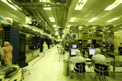
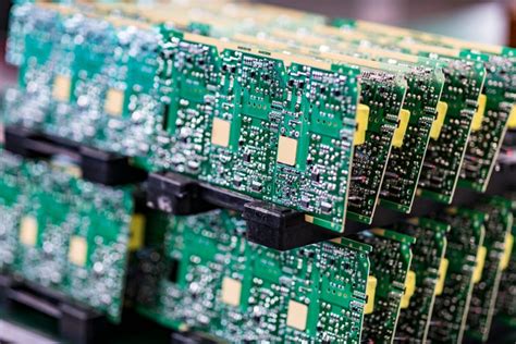
Whether PCB manufacturing utilizes simple or complex technologies, many operations in PCB engineering require wet processing and the removal of residual moisture. Raw materials used in PCB manufacturing require protection during storage, handling, and stress during the PCB assembly process. The following is a brief guide to implementing controls at each stage of PCB operation:
1.Lamination
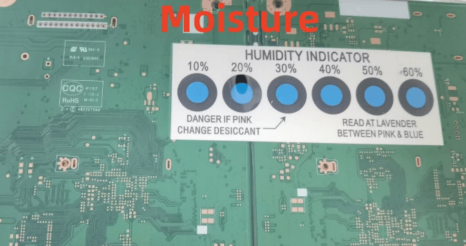
Lamination is the dehydration step in PCB manufacturing, as the core and prepreg are stacked together to bond the layers into the laminate. The primary factors to control during the lamination process are temperature, time, and heating rate. Sometimes, when dryness is low, measures are taken to reduce the vacuum level to minimize the potential for internal voids that attract moisture. Therefore, using gloves when handling prepreg can effectively control moisture levels. This reduces cross-contamination. Non-corrosive humidity indicator cards should be flexible enough to allow for adjustments to humidity levels as needed. Lamination cycles should be short, and laminates should be stored effectively in a controlled environment to help prevent moisture pockets from forming in the laminate.
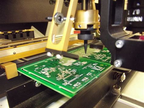
2.Post-Lamination Processes and PCB Assembly
After drilling, photolithography, and etching operations in PCB manufacturing, moisture absorption, which is trapped during wet processes, is higher. Screen printing curing and solder mask baking are steps that require careful attention to mitigate entrapped moisture. Minimizing the hold time between steps and even carefully managing storage conditions can be even more effective in reducing moisture absorption levels. Ensuring that boards are adequately dry during the early stages of PCB lamination can help reduce post-lamination baking operations. Furthermore, using high-quality surface treatments can prevent cracks during drilling, and removing residual moisture through baking before the hot-air solder leveling process. Baking times should be tailored to the desired moisture content, the complexity of the PCB manufacturing, the PCB surface finish, and the required thickness of the board.
Therefore, it is crucial to stay up-to-date on the effects of moisture in PCB manufacturing to avoid PCB failures, damage, and short circuits, which can lead to increased rework costs. Now, researchers are on the verge of unveiling a more advanced solution that could save time, energy, and costs by controlling the moisture element at every step of PCB manufacturing using eco-friendly PCB technology.