Immersion Gold PCB: A Comprehensive Guide to Surface Finishing Technology
1. Introduction
Printed Circuit Boards (PCBs) are essential components in modern electronics, providing mechanical support and electrical connections for electronic components. One critical aspect of PCB manufacturing is the surface finish, which protects the copper traces from oxidation and ensures reliable solderability. Among the various surface finishing techniques available, Immersion Gold (ENIG – Electroless Nickel Immersion Gold) has gained significant popularity due to its excellent performance in high-reliability applications.
This article explores Immersion Gold PCB technology, including its process, advantages, disadvantages, applications, and comparisons with other surface finishes.
2. What is Immersion Gold PCB?
Immersion Gold, also known as Electroless Nickel Immersion Gold (ENIG), is a two-layer metallic coating applied to PCBs. It consists of:
- Electroless Nickel (Ni) Layer (3-6 μm): Provides a barrier to prevent copper diffusion and enhances solder joint strength.
- Immersion Gold (Au) Layer (0.05-0.1 μm): Protects the nickel from oxidation and ensures excellent solderability and wire-bonding capability.
Unlike electroplated gold, immersion gold is deposited via a chemical displacement reaction, where gold ions replace nickel atoms on the surface, resulting in a thin, uniform layer.
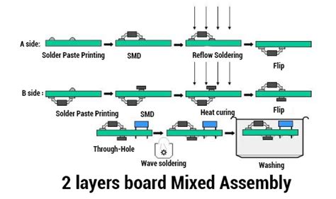
3. The Immersion Gold PCB Process
The ENIG process involves several key steps:
Step 1: Cleaning and Surface Preparation
- The PCB undergoes cleaning and micro-etching to remove oxides and contaminants from the copper surface.
Step 2: Electroless Nickel Deposition
- A nickel-phosphorus (Ni-P) layer (typically 3-6 μm thick) is deposited on the copper through an autocatalytic chemical reaction.
- The phosphorus content (usually 4-10%) influences hardness and corrosion resistance.
Step 3: Immersion Gold Plating
- The PCB is immersed in a gold solution, where gold ions displace nickel atoms, forming a thin gold layer (0.05-0.1 μm).
- This layer protects the nickel from oxidation while maintaining excellent conductivity.
Step 4: Post-Treatment and Inspection
- The PCB is rinsed and dried.
- Quality checks include thickness measurement, adhesion tests, and solderability testing.
4. Advantages of Immersion Gold PCB
Immersion Gold PCBs offer several benefits over other surface finishes:
① Excellent Oxidation Resistance
- Gold protects the underlying nickel from oxidation, ensuring long-term reliability.
② Superior Solderability
- The gold surface provides a smooth, flat finish, improving solder joint formation.
③ Suitable for Fine-Pitch Components
- ENIG is ideal for BGA, QFN, and CSP packages due to its flat surface and precise deposition.
④ Good Electrical Conductivity
- Gold’s low contact resistance makes it suitable for high-frequency and RF applications.
⑤ Wire Bonding Compatibility
- ENIG supports gold and aluminum wire bonding, making it useful in IC packaging.
⑥ RoHS Compliance
- Unlike lead-based finishes (e.g., HASL), ENIG is environmentally friendly.
5. Disadvantages of Immersion Gold PCB
Despite its advantages, ENIG has some limitations:
① Higher Cost
- Gold is expensive, making ENIG more costly than HASL or OSP.
② Risk of Black Pad Syndrome
- Improper nickel plating can lead to “black pad” defects, causing weak solder joints.
③ Thin Gold Layer Vulnerability
- The gold layer is thin and can wear off during multiple reflow cycles.
④ Not Suitable for Thick Gold Requirements
- For applications needing thick gold (e.g., edge connectors), hard gold plating (electroplated gold) is preferred.
6. Applications of Immersion Gold PCB
ENIG is widely used in high-reliability and precision electronics, including:
✅ Consumer Electronics (Smartphones, Tablets, Wearables)
✅ Medical Devices (Implantable and Diagnostic Equipment)
✅ Automotive Electronics (ECUs, Sensors, Infotainment Systems)
✅ Aerospace & Defense (Avionics, Radar Systems)
✅ Telecommunications (5G, RF Modules)
✅ Industrial Control Systems (Robotics, Automation)
7. Comparison with Other PCB Surface Finishes
| Surface Finish | Thickness | Solderability | Cost | Applications |
|---|---|---|---|---|
| Immersion Gold (ENIG) | Ni: 3-6 μm, Au: 0.05-0.1 μm | Excellent | High | High-reliability, fine-pitch |
| HASL (Hot Air Solder Leveling) | 1-25 μm | Good | Low | General-purpose PCBs |
| OSP (Organic Solderability Preservative) | 0.2-0.5 μm | Fair (short shelf life) | Low | Consumer electronics |
| Electroplated Gold (Hard Gold) | Au: 0.5-2.5 μm | Excellent | Very High | Edge connectors, wear resistance |
| Immersion Silver (IAg) | 0.1-0.3 μm | Good | Medium | High-frequency, LED PCBs |
8. Future Trends in Immersion Gold PCB Technology
- Improved Nickel Bath Formulations to reduce black pad defects.
- Selective ENIG Deposition to lower costs by gold-plating only critical areas.
- Hybrid Finishes (e.g., ENIG + OSP) for enhanced performance.
- Nanotechnology-Based Gold Deposition for ultra-thin, high-performance coatings.
9. Conclusion
Immersion Gold (ENIG) PCB surface finish is a high-performance, reliable, and versatile option for modern electronics. While it is more expensive than alternatives like HASL or OSP, its superior solderability, oxidation resistance, and fine-pitch compatibility make it indispensable in advanced applications.
As PCB technology evolves, ENIG will continue to play a crucial role in high-frequency, automotive, medical, and 5G devices, ensuring robust and long-lasting electronic connections.