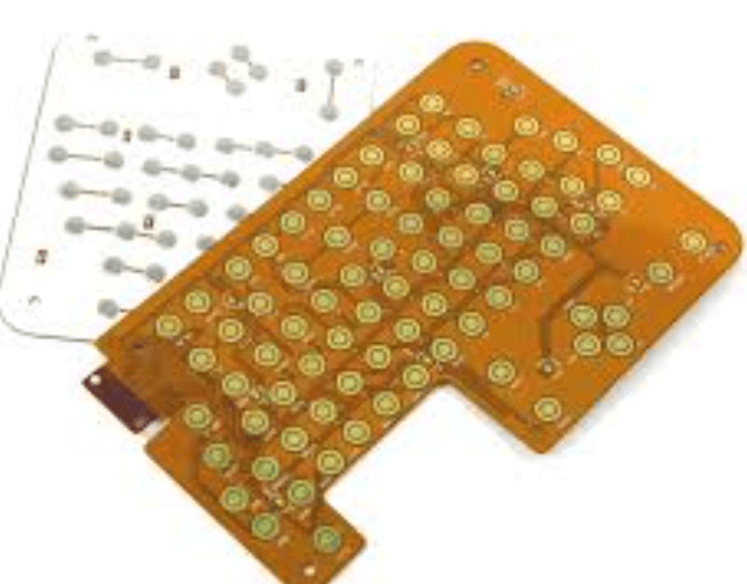
Impedance control flex pcb
Understanding Impedance Control in Flexible PCBs: Key Considerations
Impedance control in flexible printed circuit boards (PCBs) is a critical aspect of modern electronics design, particularly as devices become more compact and complex. Understanding the nuances of impedance control is essential for engineers and designers who aim to ensure signal integrity and optimal performance in their electronic products. Flexible PCBs, known for their ability to bend and conform to various shapes, present unique challenges and opportunities in the realm of impedance control.
To begin with, impedance is the measure of opposition that a circuit presents to the flow of alternating current (AC) and is a combination of resistance, inductive reactance, and capacitive reactance.
In the context of PCBs, maintaining consistent impedance is crucial for high-frequency signal transmission. Variations in impedance can lead to signal reflections, loss, and distortion, which can significantly degrade the performance of electronic devices. Therefore, controlling impedance is vital for applications such as high-speed data communication, radio frequency (RF) circuits, and other sensitive electronic systems.
Flexible PCBs, due to their inherent material properties and structural characteristics, require special attention when it comes to impedance control.
The materials used in flexible PCBs, such as polyimide and polyester, have different dielectric constants compared to traditional rigid PCB materials like FR-4. This difference affects the impedance of the traces on the PCB. Moreover, the thickness of the flexible substrate can vary, further complicating impedance calculations. Consequently, designers must carefully select materials and design parameters to achieve the desired impedance levels.
One of the key considerations in impedance control for flexible PCBs is the trace geometry.
The width, thickness, and spacing of the traces, as well as the distance to the reference plane, play a significant role in determining the impedance. Designers often use simulation tools to model and predict the impedance of various trace configurations. By adjusting these parameters, they can fine-tune the impedance to match the requirements of the specific application. Additionally, the use of controlled impedance traces, such as microstrip or stripline configurations, can help achieve the desired impedance levels.
Another important factor is the manufacturing process.
The fabrication of flexible PCBs involves different techniques compared to rigid PCBs, and these can impact the final impedance. For instance, the etching process used to create the traces can introduce variations in trace width and thickness, affecting the impedance. Therefore, close collaboration with PCB manufacturers is essential to ensure that the design specifications are met during production. Manufacturers may also offer impedance testing services to verify that the fabricated PCBs meet the required impedance standards.
Furthermore, environmental factors such as temperature and humidity can influence the impedance of flexible PCBs.
The materials used in flexible PCBs can expand or contract with changes in temperature, altering the trace dimensions and, consequently, the impedance. Designers must account for these variations during the design phase to ensure reliable performance under different operating conditions.
In conclusion, understanding and controlling impedance in flexible PCBs is a complex but essential task for ensuring the performance and reliability of modern electronic devices. By carefully considering material properties, trace geometry, manufacturing processes, and environmental factors, designers can achieve the desired impedance levels and maintain signal integrity. As technology continues to advance, the demand for flexible PCBs with precise impedance control will only grow, making this an increasingly important area of focus for the electronics industry.
Designing Flexible PCBs with Precise Impedance Control
Designing flexible printed circuit boards (PCBs) with precise impedance control is a critical aspect of modern electronics engineering, particularly as devices become more compact and complex.
The demand for flexible PCBs has surged due to their ability to conform to various shapes and fit into tight spaces, making them ideal for applications in wearable technology, medical devices, and advanced communication systems.
However, achieving precise impedance control in these flexible circuits presents unique challenges that require careful consideration and meticulous design strategies.
To begin with, understanding the concept of impedance is essential.
Impedance, in the context of PCBs, refers to the resistance that an electrical signal encounters as it travels along a trace. This resistance is influenced by several factors, including the trace width, the dielectric material, and the distance between the trace and the ground plane.
In flexible PCBs, these parameters can vary significantly due to the inherent flexibility and potential for bending and twisting, which can alter the electrical characteristics of the circuit.
One of the primary challenges in designing flexible PCBs with precise impedance control is maintaining consistent trace dimensions.
Unlike rigid PCBs, where the traces remain static, flexible PCBs can experience mechanical stress that may lead to variations in trace width and thickness. To mitigate this, designers often employ advanced simulation tools to model the mechanical behavior of the PCB under different conditions. These simulations help in predicting how the traces will behave when the PCB is bent or twisted, allowing for adjustments in the design phase to ensure that impedance remains within the desired range.
Moreover, the choice of materials plays a crucial role in impedance control.
Flexible PCBs are typically made from polyimide or polyester substrates, which offer excellent flexibility and thermal stability. However, these materials have different dielectric properties compared to the FR-4 material commonly used in rigid PCBs. Therefore, designers must carefully select materials with dielectric constants that align with the impedance requirements of the circuit. Additionally, the use of low-loss materials can help minimize signal attenuation, which is particularly important in high-frequency applications.
Another important consideration is the stack-up configuration of the flexible PCB.
The stack-up refers to the arrangement of conductive and insulating layers within the PCB. By strategically designing the stack-up, engineers can control the impedance of the traces more effectively. For instance, incorporating a ground plane close to the signal traces can help stabilize impedance by providing a consistent return path for the signals. This approach is often used in high-speed digital and RF circuits where precise impedance control is paramount.
Furthermore, the manufacturing process itself can impact impedance control.
Variations in etching, lamination, and drilling processes can introduce discrepancies in trace dimensions and layer alignment. To address this, manufacturers employ stringent quality control measures and advanced fabrication techniques to ensure that the final product adheres to the specified design parameters.
Collaboration between designers and manufacturers is essential to identify potential issues early in the process and implement solutions that maintain impedance integrity.
In conclusion, designing flexible PCBs with precise impedance control requires a comprehensive understanding of both electrical and mechanical principles.
By leveraging advanced simulation tools, selecting appropriate materials, optimizing stack-up configurations, and ensuring meticulous manufacturing processes, engineers can overcome the challenges associated with flexible PCB design. As technology continues to evolve, the ability to achieve precise impedance control in flexible circuits will remain a key factor in the development of innovative electronic devices.
The Role of Impedance Control in High-Frequency Flexible PCB Applications
In the realm of modern electronics, the demand for high-frequency applications has surged, necessitating advancements in printed circuit board (PCB) technology. Among these advancements, flexible PCBs have emerged as a pivotal innovation, offering unparalleled versatility and adaptability. However, as electronic devices become more sophisticated, the need for precise impedance control in flexible PCBs has become increasingly critical. Impedance control is essential in ensuring signal integrity, particularly in high-frequency applications where even minor deviations can lead to significant performance issues.
To understand the importance of impedance control in flexible PCBs, it is crucial to first comprehend the concept of impedance itself.
Impedance, in the context of PCBs, refers to the opposition that a circuit presents to the flow of alternating current (AC) at a particular frequency. It is a complex quantity, comprising both resistance and reactance, and is measured in ohms. In high-frequency applications, maintaining consistent impedance is vital to prevent signal reflection, distortion, and loss, which can degrade the performance of the electronic device.
Flexible PCBs, known for their ability to bend and conform to various shapes, are increasingly used in applications such as wearable technology, medical devices, and aerospace systems. These applications often operate at high frequencies, where impedance mismatches can be particularly detrimental. Therefore, achieving precise impedance control in flexible PCBs is not merely a technical challenge but a necessity for ensuring optimal functionality.
One of the primary factors influencing impedance in flexible PCBs is the dielectric material used.
The dielectric constant of the material affects the capacitance and, consequently, the impedance of the circuit. Selecting a dielectric material with a stable dielectric constant over the desired frequency range is crucial for maintaining consistent impedance. Additionally, the thickness of the dielectric layer and the width of the conductive traces play significant roles in determining the impedance. Manufacturers must carefully design and fabricate flexible PCBs to ensure that these parameters are tightly controlled.
Moreover, the layout and routing of traces on a flexible PCB can significantly impact impedance.
High-frequency signals are particularly sensitive to changes in trace geometry, such as bends and vias, which can introduce impedance discontinuities. To mitigate these effects, designers often employ techniques such as controlled trace widths, differential pair routing, and impedance matching. These strategies help maintain uniform impedance throughout the circuit, thereby preserving signal integrity.
In addition to design considerations, advanced manufacturing processes are essential for achieving precise impedance control in flexible PCBs.
Techniques such as laser direct structuring and precision etching enable manufacturers to produce intricate trace patterns with high accuracy. Furthermore, rigorous testing and quality assurance processes are employed to verify that the impedance specifications are met consistently across production batches.
In conclusion, the role of impedance control in high-frequency flexible PCB applications cannot be overstated. As electronic devices continue to evolve, the demand for reliable and efficient high-frequency performance will only increase. By understanding and addressing the factors that influence impedance, manufacturers can ensure that flexible PCBs meet the stringent requirements of modern high-frequency applications. This not only enhances the performance and reliability of electronic devices but also paves the way for further innovations in the field of flexible electronics.
Techniques for Achieving Accurate Impedance Control in Flex PCB Manufacturing
In the realm of modern electronics, flexible printed circuit boards (flex PCBs) have emerged as a pivotal component, offering unparalleled versatility and adaptability.
One of the critical aspects of flex PCB manufacturing is achieving accurate impedance control, which is essential for ensuring signal integrity and optimal performance in high-frequency applications. Impedance control in flex PCBs is a complex process that requires meticulous attention to detail and a comprehensive understanding of various influencing factors. To achieve precise impedance control, manufacturers employ a range of techniques, each contributing to the overall effectiveness of the process.
To begin with, the selection of materials plays a fundamental role in impedance control.
The dielectric constant and thickness of the substrate material significantly impact the impedance characteristics of the flex PCB. Manufacturers often opt for materials with stable dielectric properties, such as polyimide, which offer consistent performance across a wide range of frequencies. By carefully choosing the substrate material, manufacturers can establish a solid foundation for achieving the desired impedance levels.
In addition to material selection, the design of the trace geometry is another crucial factor.
The width, thickness, and spacing of the conductive traces directly influence the impedance. To maintain precise control, manufacturers utilize advanced computer-aided design (CAD) software to simulate and optimize the trace layout. This allows for the fine-tuning of trace dimensions to meet specific impedance requirements. Moreover, the use of controlled impedance traces, such as microstrip or stripline configurations, further enhances the ability to achieve accurate impedance control.
Furthermore, the manufacturing process itself must be meticulously controlled to ensure consistency and precision.
Techniques such as etching and lamination are critical in defining the final trace geometry and substrate thickness. Any variations in these processes can lead to deviations in impedance, potentially compromising the performance of the flex PCB. Therefore, manufacturers implement stringent quality control measures, including regular inspections and testing, to identify and rectify any discrepancies during production.
Another technique employed in achieving accurate impedance control is the use of impedance modeling and simulation tools.
These tools enable manufacturers to predict the impedance characteristics of a flex PCB design before it is physically produced. By simulating various design parameters and manufacturing conditions, manufacturers can identify potential issues and make necessary adjustments to ensure the final product meets the desired specifications. This proactive approach not only enhances the accuracy of impedance control but also reduces the likelihood of costly rework or redesign.
Moreover, collaboration between design engineers and manufacturing teams is essential for successful impedance control.
By fostering open communication and sharing insights, both parties can work together to address potential challenges and optimize the design for manufacturability. This collaborative approach ensures that the design intent is accurately translated into the final product, minimizing the risk of impedance-related issues.
In conclusion, achieving accurate impedance control in flex PCB manufacturing is a multifaceted process that requires careful consideration of material selection, trace geometry, manufacturing techniques, and simulation tools. By employing these techniques and fostering collaboration between design and manufacturing teams, manufacturers can ensure that flex PCBs meet the stringent performance requirements of modern electronic applications. As technology continues to advance, the importance of precise impedance control will only grow, underscoring the need for ongoing innovation and refinement in flex PCB manufacturing processes.