In-depth discussion of PCBA circuit boards
Introduction
In modern electronic devices, printed circuit boards (PCBs) and their assembly process (PCBA) are crucial components. Whether it is mobile phones, computers, home appliances or industrial equipment, almost all electronic products rely on circuit boards to realize their functions. This article will explore the concepts, processes, materials, applications and future development trends of PCBA in depth.
1.What is PCBA?
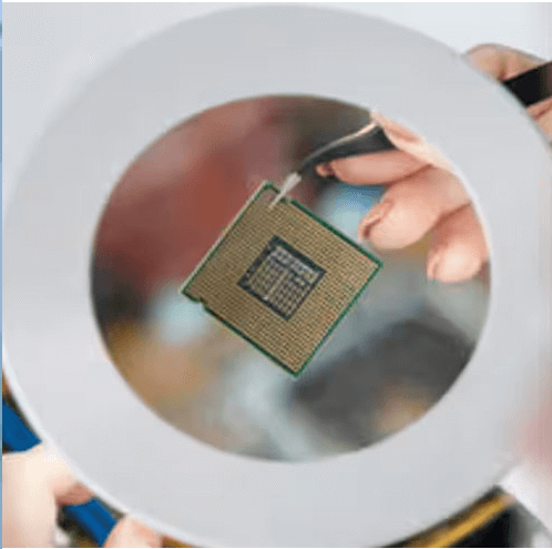
PCBA is the abbreviation of “Printed Circuit Board Assembly”, which refers to the process of soldering electronic components to printed circuit boards. This process not only includes the soldering of components, but also involves the testing and quality control of circuit boards. PCBA is a key link in the manufacture of electronic products and directly affects the performance and reliability of products.
1.1 The difference between PCB and PCBA
PCB (printed circuit board): refers to a substrate that only contains circuit patterns, usually composed of insulating materials (such as FR-4) and conductive materials (such as copper).
PCBA (circuit board assembly): is based on PCB, through welding, patch and other processes to assemble various electronic components (such as resistors, capacitors, integrated circuits, etc.) to PCB to form a complete circuit function.
2.PCBA manufacturing process
The PCBA manufacturing process usually includes the following main steps:
2.1 Design and layout
In the manufacturing process of PCBA, circuit design and layout are required first. Designers use CAD software (such as Altium Designer, Eagle, etc.) to draw circuit diagrams and layout components. After the design is completed, Gerber files are generated for subsequent PCB manufacturing.
2.2 PCB manufacturing
PCB manufacturing is the process of converting the design into an actual circuit board, which mainly includes the following steps:
Material preparation: Select suitable substrate materials (such as FR-4, CEM-1, etc.).
Graphic transfer: Transfer the circuit pattern to the substrate through photolithography technology.
Etching: Remove excess copper layer to form a circuit pattern.
Drilling: Drill holes according to design requirements for subsequent component insertion and connection.
Surface treatment: Treat the surface of the PCB to improve welding performance and corrosion resistance.
2.3 Component Mounting
Component mounting is the process of placing electronic components onto a PCB, and is usually divided into two ways:
Through-Hole: insert component pins into holes on the PCB and then solder.
Surface Mount (SMD): place components directly on the PCB surface and fix them by reflow soldering or wave soldering.
2.4 Soldering
Soldering is a key step in connecting components to PCBs. Common soldering methods include:
Reflow soldering: Applicable to surface mount components, the solder is melted and solidified by heating.
Wave soldering: Applicable to through-hole components, the PCB is passed through a wave of molten solder to complete the soldering.
2.5 Testing and Inspection
After soldering is completed, the PCBA needs to be tested to ensure its performance and reliability. Common testing methods include:
Visual inspection: Check the quality of solder joints visually or using a microscope.
Functional testing: Check whether the circuit board is working properly and whether it meets the design requirements.
Environmental testing: Test the stability and durability of the PCBA under different environmental conditions.
2.6 Packaging and Delivery
The PCBA that has passed the test will be packaged and prepared for delivery to customers or subsequent product assembly.
3.PCBA Materials
The material selection of PCBA is crucial to the performance and reliability of the circuit board. The main materials include:
3.1 Substrate Materials
FR-4: The most commonly used PCB material with good insulation properties and mechanical strength.
CEM-1/CEM-3: Suitable for low-cost and simple circuit board applications.
Polyimide: Flexible circuit boards for high-temperature and high-frequency applications.
3.2 Conductive Materials
Copper: The most commonly used conductive material with good conductivity and weldability.
Gold: Used in high-end applications with excellent corrosion resistance and conductivity.
3.3 Solder
Solder is an important material for connecting components and PCBs. Commonly used solders include tin-lead alloys and lead-free solders. Lead-free solders have gradually become mainstream under the promotion of environmental regulations.
4. Application of PCBA
PCBA is widely used in various fields, mainly including:
4.1 Consumer electronics
Such as mobile phones, tablets, TVs, etc., PCBA is the core component of these devices, which directly affects the performance and user experience of the product.
4.2 Industrial equipment
In industrial automation and control systems, PCBA is used for sensors, controllers and other equipment to ensure the stability and reliability of the equipment.
4.3 Medical equipment
Medical equipment has extremely high requirements for PCBA and must have high reliability and stability, such as heart monitors, imaging equipment, etc.
4.4 Automotive electronics
With the development of automotive intelligence, PCBA plays an increasingly important role in automotive electronic systems, such as in-vehicle navigation, automatic driving systems, etc.
5.Future development trend of PCBA
With the continuous advancement of technology, the PCBA industry is also developing continuously, and the main trends include:
5.1 Miniaturization and high density
As electronic products develop towards miniaturization and high performance, the design and manufacturing of PCBA also need to be more compact, the spacing between components is reduced, and the wiring is more complicated.
5.2 Lead-free soldering technology
The promotion of environmental protection regulations has made lead-free soldering technology gradually become mainstream. In the future, more lead-free solders and welding processes will be developed and applied.
5.3 Intelligent manufacturing
With the advancement of Industry 4.0, PCBA manufacturing will increasingly adopt intelligent technologies, such as automated production lines, IoT monitoring, etc., to improve production efficiency and quality.
5.4 Application of new materials
The continuous research and development of new materials will promote the performance improvement of PCBA, such as flexible circuit boards, high-frequency materials, etc., which will be more widely used in future electronic products.
Conclusion
As a key link in the manufacturing of electronic products, the importance of PCBA is self-evident. With the continuous advancement of science and technology, the manufacturing process, material selection and application fields of PCBA are constantly developing. Understanding the basic knowledge and future trends of PCBA is of great guiding significance for professionals and enterprises engaged in the electronics industry. Through continuous innovation and improvement, PCBA will play a greater role in future electronic products.


