Introduction to Microphone PCB Design
The Printed Circuit Board (PCB) is a fundamental component in modern electronics, serving as the backbone for connecting various electronic components. In the context of microphones, the PCB plays a crucial role in ensuring the device’s functionality, reliability, and performance. This article delves into the intricacies of microphone PCB design, covering aspects such as layout considerations, material selection, signal integrity, and manufacturing processes.
1. Understanding the Role of PCB in Microphones
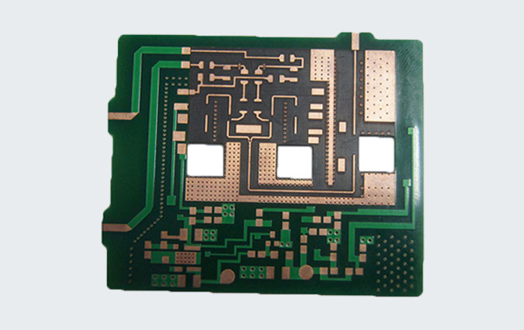
Microphones are transducers that convert sound waves into electrical signals. The PCB in a microphone is responsible for housing and connecting the electronic components that process these signals. These components may include preamplifiers, analog-to-digital converters (ADCs), and other signal conditioning circuits. The design of the PCB must ensure that the electrical signals are accurately captured, processed, and transmitted without significant loss or interference.
2. Key Considerations in Microphone PCB Design
2.1. Layout Considerations
The layout of a microphone PCB is critical to its performance. Proper placement of components, routing of traces, and grounding strategies are essential to minimize noise and interference. Here are some key layout considerations:
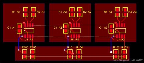
- Component Placement: Components should be placed in a way that minimizes the length of signal paths. This reduces the risk of signal degradation and interference. For instance, the microphone capsule should be placed close to the preamplifier to minimize the distance the signal travels.
- Trace Routing: Signal traces should be as short and direct as possible. High-frequency signals are particularly susceptible to interference, so it’s important to avoid long, meandering traces. Differential signaling can be used to reduce noise in sensitive audio signals.
- Grounding: Proper grounding is essential to minimize noise and ensure signal integrity. A solid ground plane is typically used to provide a low-impedance return path for signals. It’s also important to separate analog and digital grounds to prevent noise from digital circuits from affecting the analog audio signals.
- Power Supply Decoupling: Decoupling capacitors should be placed close to the power pins of active components to filter out high-frequency noise from the power supply. This helps maintain a stable voltage supply and reduces the risk of noise being introduced into the audio signal.
2.2. Material Selection
The choice of materials for the PCB can significantly impact the performance of the microphone. Key factors to consider include:
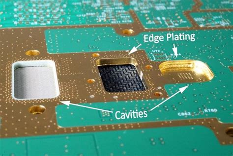
- Substrate Material: The substrate material affects the electrical properties of the PCB, such as dielectric constant and loss tangent. Common materials include FR-4, which is widely used for its balance of cost and performance, and high-frequency laminates like Rogers materials, which offer better performance for high-frequency applications.
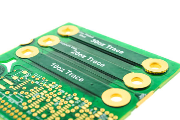
- Copper Thickness: The thickness of the copper traces affects the current-carrying capacity and the impedance of the traces. Thicker copper can handle higher currents but may increase the cost and complexity of the PCB.
- Surface Finish: The surface finish affects the solderability and durability of the PCB. Common finishes include HASL (Hot Air Solder Leveling), ENIG (Electroless Nickel Immersion Gold), and OSP (Organic Solderability Preservative). ENIG is often preferred for its flat surface and good solderability, which is important for fine-pitch components.
2.3. Signal Integrity
Maintaining signal integrity is crucial in microphone PCB design, as any noise or distortion can degrade the audio quality. Key considerations include:
- Impedance Matching: Proper impedance matching between the microphone capsule, preamplifier, and other components is essential to prevent signal reflections and loss. This is particularly important in high-frequency applications.
- Shielding: Shielding can be used to protect sensitive audio signals from electromagnetic interference (EMI). This can be achieved through the use of grounded copper pours, shielded cables, and metal enclosures.
- Noise Reduction Techniques: Techniques such as differential signaling, filtering, and careful layout can help reduce noise in the audio signal. For example, using a differential pair for the audio signal can cancel out common-mode noise.
2.4. Thermal Management
Microphone PCBs, especially those used in high-power applications, need to manage heat effectively to ensure reliable operation. Key considerations include:
- Thermal Vias: Thermal vias can be used to transfer heat from components to the ground plane or other heat-dissipating structures. This helps prevent overheating and ensures stable operation.
- Heat Sinks: In some cases, heat sinks may be required to dissipate heat from high-power components. The PCB layout should accommodate the placement of heat sinks and ensure adequate airflow.
3. Manufacturing Processes
The manufacturing process for microphone PCBs involves several steps, each of which must be carefully controlled to ensure quality and reliability. Key steps include:
- PCB Fabrication: The PCB is fabricated by laminating layers of substrate material and copper, then etching away unwanted copper to create the circuit traces. The process involves drilling holes for vias and component leads, and applying the surface finish.
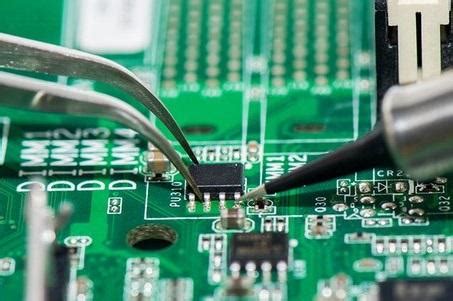
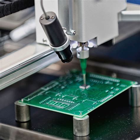
- Component Assembly: Components are placed on the PCB using automated pick-and-place machines, then soldered using reflow or wave soldering techniques. For high-density designs, surface-mount technology (SMT) is commonly used.
- Testing and Inspection: After assembly, the PCB is tested to ensure it functions correctly. This may involve electrical testing, visual inspection, and functional testing of the microphone.
4. Advanced Topics in Microphone PCB Design
4.1. Miniaturization
As consumer electronics continue to shrink in size, there is a growing demand for smaller, more compact microphone PCBs. Miniaturization presents several challenges, including:
- High-Density Interconnects: Achieving high-density interconnects requires advanced PCB fabrication techniques, such as microvias and fine-pitch components. This can increase the complexity and cost of the PCB.
- Thermal Management: Smaller PCBs have less surface area for heat dissipation, making thermal management more challenging. Techniques such as thermal vias and heat sinks become even more critical.
4.2. Flexible PCBs
Flexible PCBs offer several advantages for microphone applications, including the ability to conform to irregular shapes and reduce the overall size of the device. However, designing flexible PCBs requires careful consideration of:
- Material Selection: Flexible PCBs use materials like polyimide, which can bend and flex without breaking. The choice of materials affects the flexibility, durability, and electrical performance of the PCB.
- Mechanical Stress: Flexible PCBs are subject to mechanical stress during bending and flexing. The design must account for this stress to prevent cracking or failure of the traces.
4.3. Integration with Other Technologies
Microphone PCBs are often integrated with other technologies, such as wireless communication modules or digital signal processing (DSP) chips. This integration presents several challenges, including:
- Signal Integrity: Integrating multiple technologies on a single PCB can increase the risk of signal interference. Careful layout and shielding are essential to maintain signal integrity.
- Power Management: Different components may have different power requirements, necessitating careful design of the power distribution network.
5. Conclusion
The design of a microphone PCB is a complex process that requires careful consideration of various factors, including layout, material selection, signal integrity, and thermal management. As technology continues to advance, new challenges and opportunities will arise, such as miniaturization, flexible PCBs, and integration with other technologies. By understanding these challenges and applying best practices in PCB design, engineers can create high-performance microphones that meet the demands of modern applications.
In summary, the PCB is a critical component in microphone design, and its performance directly impacts the quality and reliability of the audio signal. As such, careful attention to detail in the design and manufacturing process is essential to ensure the success of the final product.