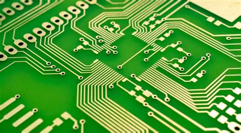
Introduction to PCB double-sided reflow process (SMT)
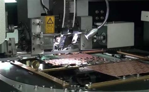
Circuit board assembly technology, now popular in the industry is full-board reflow soldering (Reflow), this technology can be divided into single-panel reflow and double-panel reflow. Single-sided reflow is used less because double-sided reflow saves board space.
Double-sided reflow requires two reflows. Because of the limitations of the process, some problems may occur.
For example, when the board goes to the second reflow furnace, the parts on the first side will fall due to gravity, especially The board flows to the furnace where the reflow zone is hot. So, what should you think about when manufacturing double-sided reflow? Which SMD parts should be placed on the first side of the reflow oven?
First of all, the smaller parts are recommended to be placed on the first side of the reflow oven
because the deformation of the PCB will be smaller when the first side passes through the reflow oven, and the precision of the solder paste printing will be higher, so it is better placed Smaller parts. Second, the smaller parts do not risk falling when the second reflow oven is over. Because the first surface part will be placed directly on the bottom surface of the circuit board when facing the second side, when the board enters the high temperature of the reflow area, it will not fall off the board because of excessive weight. For more information on designing PCBs, please visit ANDWIN CIRCUITS CO.,LTD. Again, the parts on the first panel must pass through the reflow oven twice, so the temperature resistance must be able to withstand the temperature of two reflows. The general resistance and capacitance are usually required to be reflowed at least three times, in order to meet the requirements. Some boards may require a re-return to the furnace because of the maintenance relationship.
Which SMD parts should be placed on the second side of the reflow oven?
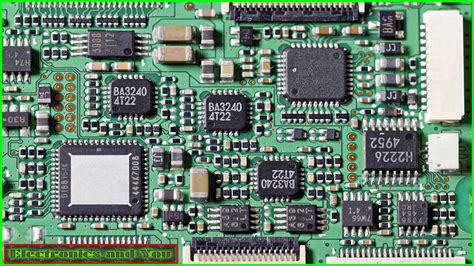
1. Large components or heavier components should be placed on the second side to prevent the parts from falling back into the furnace.
LGA and BGA parts should be placed on the second side of the furnace as much as possible, so as to avoid the unnecessary risk of re-soldering during the second pass to reduce the chance of empty/false welding. If there are small and small BGA parts, it can also be placed on the first side of the reflow oven, as long as it can effectively avoid PCB deformation.
2, parts can not withstand too much high temperature parts should be placed on the second side of the reflow oven, this is to avoid parts too much temperature and damage.
PIH/PIP parts should also be placed on the second side of the furnace, unless the length of the solder fillet does not exceed the thickness of the board, otherwise the foot that protrudes from the surface of the PCB will interfere with the steel sheet on the second side, which will make the second side The solder paste printed steel plate cannot be flat on the PCB, which causes the solder paste to print abnormally.
3. Some components may have soldering work inside.
For example, a cable connector with LED lights must pay attention to whether the temperature resistance of such parts can pass through the reflowing furnace twice. If it is not possible, it must be placed on the second side. Pieces.
Only when the parts are placed on the second side of the patch to pass the reflow oven, it means that the circuit board has passed the high temperature baptism of the reflow oven. At this time, the circuit board has some warpage and deformation, that is, tin. The amount of paste printed and the position of printing will become more difficult to control, so it will easily cause problems such as empty welding or short circuit. Therefore, it is recommended to place 0201 and fine feet in the parts of the second side. For pitch parts, the BGA should also try to choose a solder ball with a larger diameter.
At present, the welding process of the circuit board can be roughly divided into full-plate welding and partial welding. The full-board welding is roughly divided into reflow soldering and wave soldering (Wave Soldering), while the board is partially soldered with carrier wave soldering ( Carrier Wave Soldering), Selective Wave Soldering, Laser Soldering, etc.
PCB board impedance board definition
First, the printed circuit board impedance characteristics:
According to the theory of signal transmission, the signal is a function of time and distance variables, so each part of the signal may change on the line. Therefore, the AC impedance of the connection, that is, the ratio of the change of the voltage to the change of the current is determined as the characteristic impedance of the transmission line:
the characteristic impedance of the transmission line is only related to the characteristics of the signal connection itself.
In the actual circuit, the resistance value of the wire itself is smaller than the distributed impedance of the system. In the high-frequency circuit, the characteristic impedance mainly depends on the distributed capacitance of the unit distributed capacitance and the unit distributed inductance. The characteristic impedance of an ideal transmission line depends only on the unit distribution capacitance of the connection and the unit distribution inductance.
Second, the calculation of the characteristic impedance of the printed circuit board:
The proportional relationship between the rising edge time of the signal and the time required for the signal to be transmitted to the receiving end determines whether the signal connection is considered to be the transmission line.
The specific proportional relationship can be explained by the following formula: If the length of the wire connection on the PCB is greater than l/b, the connecting wire between the signals can be regarded as the transmission line.
According to the calculation formula of the equivalent impedance of the signal, the impedance of the transmission line can be expressed by the following formula: wL>>R is satisfied in the case of high frequency (tens of megahertz to several hundred megahertz) (of course, in the range where the signal frequency is greater than 109 Hz, Considering the skin effect of the signal, this relationship needs to be carefully studied).
Then for a certain transmission line, its characteristic impedance is a constant. The reflection phenomenon of the signal is caused by the inconsistency between the characteristic impedance of the driving end of the signal and the transmission line and the impedance of the receiving end. For a CMOS circuit, the output impedance of the driver end of the signal is relatively small, tens of ohms. The input impedance of the receiving end is relatively large.
Third, printed circuit board characteristic impedance control:
The characteristic impedance of the conductor on the printed circuit board is an important indicator of the circuit design. Especially in the PCB design of the high frequency circuit, it must be considered whether the characteristic impedance of the wire and the characteristic impedance required by the device or signal are consistent and matched. Therefore, there are two concepts that must be noted in the reliability design of PCB design.
Fourth, printed circuit board impedance control:
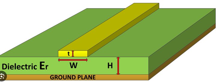
There are various signal transmissions in the conductors in the circuit board. When the transmission frequency must be increased, the frequency must be increased. If the circuit itself is different due to etching, laminate thickness, wire width, etc., the impedance value will be changed. Signal distortion. Therefore, the conductor on the high-speed circuit board, the impedance value should be controlled within a certain range, called “impedance control.” The factors affecting the impedance of the PCB trace are mainly the width of the copper wire, the thickness of the copper wire, the dielectric constant of the medium, the thickness of the medium, the thickness of the pad, the path of the ground line, and the trace around the trace. Therefore, when designing the PCB, the impedance of the board trace must be controlled to avoid signal reflection and other electromagnetic interference and signal integrity problems as much as possible to ensure the stability of the actual use of the PCB board. The calculation method of the microstrip line and stripline impedance on the PCB can refer to the corresponding empirical formula.
Fifth, the printed circuit board impedance matching:
In the circuit board, if there is a signal transmission, it is desirable to be smoothly transmitted to the receiving end from the emitting end of the power source with minimal energy loss, and the receiving end completely absorbs it without any reflection. To achieve this type of transmission, the impedance in the line must be equal to the impedance inside the emitting end to be called “impedance matching.” Impedance matching is one of the design elements when designing high speed PCB circuits.
The impedance value has an absolute relationship with the routing method.
For example, whether the distance between the surface layer (Microstrip) or the inner layer (Stripline/Double Stripline), the reference power layer or the ground layer, the trace width, and the PCB material affect the characteristic impedance of the trace. That is to say, the impedance value can be determined after wiring, and the characteristic impedance produced by different PCB manufacturers is also slightly different. General simulation software can not consider some discontinuous wiring conditions due to the limitation of the circuit model or the mathematical algorithm used. At this time, only some terminators (Temninators), such as series resistors, can be reserved on the schematic. Moderate the effect of discontinuity in the trace impedance. The only way to solve the problem is to pay attention to avoiding impedance discontinuities.