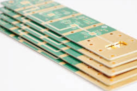
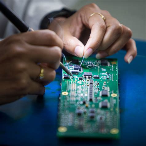
Jet pcb assembly
Benefits Of Automated Jet PCB Assembly
Automated jet PCB assembly has revolutionized the electronics manufacturing industry, offering a multitude of benefits that enhance efficiency, precision, and overall product quality.
One of the primary advantages of this technology is its ability to significantly reduce production time.
Traditional methods of PCB assembly often involve manual soldering and placement of components, which can be time-consuming and prone to human error. In contrast, automated jet PCB assembly utilizes advanced machinery to place and solder components with remarkable speed and accuracy, thereby accelerating the entire manufacturing process.
Moreover, the precision offered by automated jet PCB assembly is unparalleled.
The technology employs sophisticated software and high-resolution cameras to ensure that each component is placed exactly where it needs to be. This level of accuracy is particularly crucial for modern electronic devices, which often feature densely packed components and intricate circuit designs. By minimizing the risk of misalignment and soldering defects, automated jet PCB assembly enhances the reliability and performance of the final product.
In addition to speed and precision, automated jet PCB assembly also offers significant cost savings.
While the initial investment in automated machinery can be substantial, the long-term benefits far outweigh the costs. Automation reduces the need for manual labor, thereby lowering labor costs and minimizing the risk of human error, which can lead to costly rework and repairs. Furthermore, the efficiency of automated systems allows for higher production volumes, enabling manufacturers to achieve economies of scale and reduce per-unit costs.
Another notable benefit of automated jet PCB assembly is its flexibility.
Traditional assembly methods often require custom tooling and fixtures for different PCB designs, which can be both time-consuming and expensive. In contrast, automated systems can be easily reprogrammed to accommodate various designs and component configurations, making it easier for manufacturers to adapt to changing market demands and customer requirements. This flexibility is particularly advantageous in industries characterized by rapid technological advancements and frequent product updates.
Environmental sustainability is another area where automated jet PCB assembly excels.
The precision and efficiency of automated systems result in less material waste, as components are placed and soldered with minimal excess. Additionally, the reduced need for manual intervention means fewer errors and less rework, further decreasing waste and conserving resources. By adopting automated jet PCB assembly, manufacturers can contribute to more sustainable production practices and reduce their environmental footprint.
Furthermore, automated jet PCB assembly enhances quality control and traceability.
Advanced software systems can monitor and record every step of the assembly process, providing detailed data on component placement, soldering quality, and overall production performance. This data can be used to identify and address potential issues before they escalate, ensuring that each PCB meets stringent quality standards. Enhanced traceability also facilitates compliance with industry regulations and customer requirements, providing manufacturers with a competitive edge in the market.
In conclusion, the benefits of automated jet PCB assembly are manifold,
encompassing increased production speed, unparalleled precision, significant cost savings, enhanced flexibility, environmental sustainability, and improved quality control. As the electronics industry continues to evolve, the adoption of automated jet PCB assembly will undoubtedly play a crucial role in driving innovation and maintaining high standards of excellence. By leveraging this advanced technology, manufacturers can not only meet the growing demands of the market but also achieve greater efficiency and sustainability in their production processes.

Key Challenges In Jet PCB Assembly And How To Overcome Them
Jet PCB assembly, a critical process in the manufacturing of printed circuit boards, involves numerous intricate steps that require precision and expertise. Despite advancements in technology, several key challenges persist in this domain, necessitating innovative solutions to ensure efficiency and reliability. Understanding these challenges and the strategies to overcome them is essential for maintaining high standards in PCB production.
One of the foremost challenges in jet PCB assembly is the accurate placement of components
Given the miniaturization trend in electronics, components are becoming increasingly smaller, making precise placement more difficult. Misalignment can lead to functional failures or reduced performance of the final product. To address this issue, manufacturers are investing in advanced pick-and-place machines equipped with high-resolution cameras and sophisticated algorithms. These machines can detect and correct placement errors in real-time, significantly enhancing accuracy.
Another significant challenge is solder paste application.
The uniform deposition of solder paste is crucial for creating reliable solder joints. Variations in paste volume can result in weak connections or short circuits. To mitigate this problem, jet printing technology is employed, which allows for precise control over the amount of solder paste deposited on each pad. This method not only improves consistency but also reduces waste, contributing to cost efficiency.
Thermal management during the reflow soldering process presents another hurdle.
The reflow process involves heating the entire PCB assembly to melt the solder paste and form solid joints. However, different components have varying thermal sensitivities, and improper temperature profiles can damage sensitive parts or lead to incomplete soldering. Advanced reflow ovens with multiple heating zones and precise temperature control are essential to ensure that each component is subjected to the appropriate thermal conditions. Additionally, thermal profiling tools can be used to monitor and adjust the temperature profile in real-time, ensuring optimal results.
Component availability and supply chain management also pose significant challenges.
The global electronics industry often faces shortages of critical components, leading to production delays and increased costs. To overcome this, manufacturers are adopting strategies such as maintaining buffer stocks, diversifying their supplier base, and using alternative components where possible. Furthermore, robust supply chain management systems that provide real-time visibility into inventory levels and lead times can help in proactive planning and risk mitigation.
Quality control is another critical aspect that cannot be overlooked.
Defects in PCB assemblies can lead to costly recalls and damage to a company’s reputation. Implementing stringent quality control measures, such as automated optical inspection (AOI) and X-ray inspection, can help detect defects early in the production process. These technologies enable the identification of issues such as solder joint defects, component misalignment, and internal structural flaws, ensuring that only high-quality products reach the market.
Finally, the rapid pace of technological advancements necessitates continuous learning and adaptation.
Engineers and technicians must stay abreast of the latest developments in materials, processes, and equipment. Regular training programs and participation in industry conferences and workshops can help professionals keep their skills updated and apply best practices in their work.
In conclusion, while jet PCB assembly presents several challenges, a combination of advanced technology, strategic planning, and continuous learning can effectively address these issues. By investing in precision equipment, optimizing thermal management, ensuring robust supply chain practices, and maintaining stringent quality control, manufacturers can overcome these challenges and achieve high standards of efficiency and reliability in PCB production.
Innovations In Jet PCB Assembly Technology
Jet PCB assembly technology has undergone significant advancements in recent years, revolutionizing the electronics manufacturing industry. This innovative approach to printed circuit board (PCB) assembly leverages state-of-the-art techniques to enhance precision, efficiency, and reliability. As the demand for more complex and compact electronic devices continues to grow, the need for advanced PCB assembly methods becomes increasingly critical. Consequently, jet PCB assembly has emerged as a pivotal solution, addressing many of the challenges faced by traditional assembly processes.
One of the most notable innovations in jet PCB assembly technology is the introduction of jet printing for solder paste deposition.
Unlike conventional stencil printing, which can be limited by the intricacies of fine-pitch components and complex board designs, jet printing offers unparalleled accuracy and flexibility. By utilizing a non-contact method to deposit solder paste, jet printing can achieve precise placement even on the smallest pads, thereby reducing the risk of defects such as bridging and insufficient solder. This advancement not only improves the overall quality of the assembled PCBs but also enhances the yield rates, making the manufacturing process more cost-effective.
In addition to solder paste deposition, jet PCB assembly technology has also seen significant improvements in component placement.
Modern jetting systems are equipped with high-speed, high-precision placement heads that can handle a wide range of component sizes and types. These systems are capable of placing components at incredibly high speeds without compromising accuracy, thanks to advanced vision systems and sophisticated algorithms. The ability to place components with such precision is particularly beneficial for the assembly of high-density interconnect (HDI) boards, which are becoming increasingly prevalent in the industry.
Moreover, the integration of automated optical inspection (AOI) systems within jet PCB assembly lines has further enhanced the reliability and quality control of the manufacturing process.
AOI systems utilize high-resolution cameras and advanced image processing software to inspect each assembled PCB for defects such as misaligned components, solder joint issues, and other anomalies. By identifying and addressing these defects early in the production process, manufacturers can significantly reduce the incidence of faulty products reaching the market, thereby improving customer satisfaction and reducing warranty costs.
Another key innovation in jet PCB assembly technology is the development of advanced materials and processes that support the assembly of flexible and rigid-flex PCBs.
These types of PCBs are increasingly used in applications where space constraints and mechanical flexibility are critical, such as in wearable devices and medical implants. Jet PCB assembly techniques have been adapted to accommodate the unique challenges posed by these materials, ensuring reliable and robust connections even in the most demanding environments.
Furthermore, the advent of Industry 4.0 and the Internet of Things (IoT) has driven the adoption of smart manufacturing practices within jet PCB assembly.
By leveraging real-time data analytics, machine learning, and interconnected systems, manufacturers can optimize their production processes, predict maintenance needs, and enhance overall operational efficiency. This shift towards a more data-driven approach not only improves the performance of jet PCB assembly lines but also enables greater customization and faster time-to-market for new products.
In conclusion, the innovations in jet PCB assembly technology have significantly transformed the electronics manufacturing landscape. Through advancements in solder paste deposition, component placement, quality control, and the integration of smart manufacturing practices, jet PCB assembly has set new standards for precision, efficiency, and reliability. As the industry continues to evolve, it is expected that these technologies will play an increasingly vital role in meeting the growing demands for more sophisticated and compact electronic devices.
Quality Control Techniques In Jet PCB Assembly
In the realm of jet PCB assembly, quality control is paramount to ensure the reliability and functionality of the final product. The intricate nature of printed circuit boards (PCBs) necessitates a meticulous approach to quality control, encompassing various techniques and methodologies. These techniques are designed to identify and rectify potential defects at every stage of the assembly process, thereby guaranteeing that the end product meets stringent industry standards.
One of the primary quality control techniques employed in jet PCB assembly is Automated Optical Inspection (AOI).
AOI systems utilize high-resolution cameras to capture detailed images of the PCB. These images are then analyzed using sophisticated algorithms to detect anomalies such as soldering defects, component misalignments, and missing components. By providing real-time feedback, AOI systems enable immediate corrective actions, thus minimizing the risk of defective boards progressing through the assembly line.
In addition to AOI, X-ray inspection is another critical quality control technique.
This method is particularly effective for identifying hidden defects that are not visible to the naked eye or through optical inspection. X-ray inspection is invaluable for examining solder joints, especially in components with Ball Grid Arrays (BGAs) where the solder connections are located beneath the component. By penetrating the layers of the PCB, X-ray inspection can reveal voids, cracks, and other imperfections that could compromise the board’s performance.
Furthermore, In-Circuit Testing (ICT) plays a crucial role in ensuring the electrical integrity of the assembled PCB.
ICT involves the use of a bed-of-nails tester to make contact with various test points on the PCB. This allows for the verification of electrical connections, component values, and signal integrity. ICT is highly effective in detecting issues such as open circuits, short circuits, and incorrect component placements. By identifying these issues early in the assembly process, ICT helps prevent costly rework and ensures that only fully functional boards proceed to the next stage.
Another essential quality control technique is Functional Testing (FT).
Unlike ICT, which focuses on individual components and connections, FT evaluates the overall functionality of the assembled PCB. This involves simulating the board’s operational environment and verifying that it performs as intended. Functional testing can uncover issues related to firmware, software, and system-level interactions that might not be detected through other inspection methods. By ensuring that the PCB operates correctly under real-world conditions, functional testing provides an additional layer of assurance regarding the board’s quality.
Moreover, Statistical Process Control (SPC) is a proactive quality control technique that monitors the assembly process itself.
SPC involves the collection and analysis of data from various stages of the assembly line to identify trends and variations. By applying statistical methods, SPC can detect deviations from established process parameters, enabling timely interventions to prevent defects. This continuous monitoring and adjustment help maintain a consistent level of quality throughout the production run.
In conclusion, the quality control techniques employed in jet PCB assembly are multifaceted and complementary, each addressing different aspects of the assembly process. Automated Optical Inspection, X-ray inspection, In-Circuit Testing, Functional Testing, and Statistical Process Control collectively ensure that the final product meets the highest standards of reliability and performance. By integrating these techniques into the assembly workflow, manufacturers can achieve a robust quality control system that minimizes defects, reduces rework, and enhances customer satisfaction.


