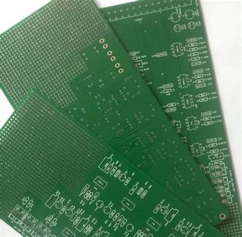
Kyocera ceramic pcb
Advantages Of Using Kyocera Ceramic PCBs In High-Frequency Applications
Kyocera ceramic printed circuit boards (PCBs) have emerged as a pivotal component in high-frequency applications, offering a range of advantages that make them indispensable in various advanced technological fields. As the demand for high-performance electronic devices continues to escalate, the need for materials that can withstand rigorous conditions while maintaining optimal functionality becomes increasingly critical. In this context, Kyocera ceramic PCBs stand out due to their unique properties and capabilities.
One of the primary advantages of Kyocera ceramic PCBs is their exceptional thermal conductivity.
Unlike traditional PCB materials, ceramics can efficiently dissipate heat, which is crucial in high-frequency applications where excessive heat generation can lead to performance degradation or even failure. This thermal management capability ensures that electronic components operate within safe temperature ranges, thereby enhancing the reliability and longevity of the devices. Furthermore, the superior thermal properties of ceramic materials reduce the need for additional cooling mechanisms, which can simplify design and reduce overall system costs.
In addition to thermal management, Kyocera ceramic PCBs offer excellent electrical insulation.
This characteristic is particularly important in high-frequency applications where signal integrity is paramount. The dielectric properties of ceramic materials minimize signal loss and crosstalk, ensuring that high-frequency signals are transmitted with minimal distortion. This results in improved performance and efficiency, making Kyocera ceramic PCBs ideal for applications such as telecommunications, aerospace, and advanced computing systems where precision and reliability are essential.
Moreover, the mechanical strength and durability of Kyocera ceramic PCBs provide a significant advantage in environments that are subject to mechanical stress or harsh conditions.
Ceramics are inherently robust and resistant to wear and tear, which makes them suitable for use in applications that require long-term stability and resilience. This durability translates to reduced maintenance and replacement costs, as the boards are less likely to suffer from physical damage over time.
Another noteworthy benefit of Kyocera ceramic PCBs is their ability to support miniaturization.
As electronic devices become increasingly compact, the need for smaller, yet more powerful components becomes evident. Ceramic PCBs can be manufactured with high precision and can accommodate complex circuit designs within a limited space. This capability is particularly advantageous in the development of portable and wearable technologies, where space constraints are a significant consideration.
Furthermore, Kyocera’s expertise in ceramic technology allows for customization and flexibility in PCB design.
This adaptability enables engineers to tailor the properties of the ceramic material to meet specific application requirements, such as adjusting the thermal expansion coefficient to match other components in the system. Such customization ensures optimal performance and integration within diverse technological ecosystems.
In conclusion, the advantages of using Kyocera ceramic PCBs in high-frequency applications are manifold. Their superior thermal conductivity, electrical insulation, mechanical strength, and support for miniaturization make them an ideal choice for a wide range of advanced applications. As technology continues to evolve, the demand for reliable and efficient materials like Kyocera ceramic PCBs is likely to grow, underscoring their importance in the future of high-frequency electronic systems. Through their innovative properties and adaptability, these ceramic PCBs are poised to play a crucial role in shaping the next generation of electronic devices.
The Role Of Kyocera Ceramic PCBs In Enhancing Thermal Management
Kyocera ceramic PCBs have emerged as a pivotal component in the realm of electronic devices, particularly in enhancing thermal management. As electronic devices become increasingly compact and powerful, the need for efficient heat dissipation has become more critical than ever. This is where Kyocera ceramic PCBs play a significant role, offering superior thermal management solutions that are essential for the optimal performance and longevity of modern electronics.
To begin with, the unique properties of ceramic materials make them an ideal choice for PCBs in high-performance applications.
Unlike traditional materials such as FR-4, ceramics possess excellent thermal conductivity, which is crucial for dissipating heat away from sensitive electronic components. This characteristic is particularly beneficial in applications where high power densities are involved, such as in power electronics, LED lighting, and RF modules. By efficiently managing heat, Kyocera ceramic PCBs help prevent overheating, thereby reducing the risk of component failure and extending the lifespan of the device.
Moreover, the thermal stability of ceramic materials ensures that Kyocera ceramic PCBs maintain their performance across a wide range of temperatures.
This is especially important in industries such as aerospace and automotive, where electronic systems are often exposed to extreme environmental conditions. The ability of ceramic PCBs to withstand high temperatures without degrading ensures reliable operation, which is a critical requirement in these demanding applications. Furthermore, the inherent rigidity and mechanical strength of ceramics provide additional benefits, including resistance to mechanical stress and vibration, which are common in harsh operating environments.
In addition to their thermal and mechanical advantages, Kyocera ceramic PCBs also offer excellent electrical insulation properties.
This is particularly advantageous in high-frequency applications, where minimizing signal loss and interference is paramount. The low dielectric constant and loss tangent of ceramic materials contribute to improved signal integrity, making them suitable for use in advanced communication systems and high-speed digital circuits. As a result, devices equipped with Kyocera ceramic PCBs can achieve higher performance levels, with faster data transmission and reduced signal distortion.
Furthermore, the versatility of Kyocera ceramic PCBs extends to their compatibility with various manufacturing processes.
They can be easily integrated into existing production lines, allowing for seamless adoption in diverse applications. The ability to support advanced packaging technologies, such as chip-on-board and multi-chip modules, further enhances their appeal in the electronics industry. This adaptability ensures that Kyocera ceramic PCBs can meet the evolving demands of modern electronic devices, providing a reliable and efficient solution for thermal management challenges.
In conclusion, the role of Kyocera ceramic PCBs in enhancing thermal management cannot be overstated.
Their superior thermal conductivity, stability, and electrical insulation properties make them an indispensable component in high-performance electronic applications. As the demand for more powerful and compact devices continues to grow, the importance of effective thermal management solutions will only increase. Kyocera ceramic PCBs, with their unique combination of properties, are well-positioned to meet these challenges, ensuring the reliable operation and longevity of electronic devices across various industries. Through their continued innovation and development, Kyocera remains at the forefront of providing cutting-edge solutions that address the critical needs of thermal management in the ever-evolving world of electronics.
Innovations In Kyocera Ceramic PCB Manufacturing Techniques
Kyocera, a leader in the field of advanced ceramics, has made significant strides in the development and manufacturing of ceramic printed circuit boards (PCBs). These innovations have positioned Kyocera at the forefront of the electronics industry, particularly in applications requiring high thermal conductivity, mechanical strength, and reliability. The advancements in Kyocera’s ceramic PCB manufacturing techniques are driven by the increasing demand for miniaturization and enhanced performance in electronic devices, which necessitate materials that can withstand extreme conditions while maintaining superior functionality.
One of the key innovations in Kyocera’s ceramic PCB manufacturing is the use of advanced ceramic materials, such as alumina and aluminum nitride.
These materials are chosen for their excellent thermal properties, which are crucial for dissipating heat in high-power applications. The ability to efficiently manage heat is essential in preventing overheating and ensuring the longevity of electronic components. Moreover, the mechanical robustness of these ceramics makes them ideal for use in environments subject to physical stress and vibration, such as automotive and aerospace applications.
In addition to material selection, Kyocera has refined its manufacturing processes to enhance the performance and reliability of ceramic PCBs.
The company employs state-of-the-art techniques such as tape casting and multilayer lamination, which allow for the precise control of thickness and layer composition. This precision is vital for achieving the desired electrical characteristics and ensuring consistent performance across different batches of PCBs. Furthermore, these techniques enable the integration of complex circuitry within a compact form factor, meeting the industry’s demand for smaller and more efficient electronic devices.
Another significant advancement in Kyocera’s manufacturing techniques is the implementation of laser drilling and cutting technologies.
These technologies provide unparalleled accuracy in creating vias and cutting board outlines, which are essential for the interconnection of different layers within a multilayer PCB. The use of lasers not only improves the precision of these processes but also reduces the risk of damage to the ceramic material, thereby enhancing the overall reliability of the final product. This level of precision is particularly important in applications where even minor defects can lead to significant performance issues.
Moreover, Kyocera has embraced the use of advanced metallization techniques to improve the electrical conductivity of ceramic PCBs.
By employing methods such as direct copper bonding and thick film technology, Kyocera ensures that the conductive pathways within the PCB are capable of handling high current loads without degradation. These metallization techniques also contribute to the overall durability of the PCB, as they provide strong adhesion between the ceramic substrate and the conductive materials.
In conclusion, Kyocera’s innovations in ceramic PCB manufacturing techniques have set a new standard in the electronics industry. By leveraging advanced materials, precise manufacturing processes, and cutting-edge technologies, Kyocera has developed ceramic PCBs that meet the rigorous demands of modern electronic applications. These advancements not only enhance the performance and reliability of electronic devices but also pave the way for future innovations in the field. As the demand for high-performance, miniaturized electronics continues to grow, Kyocera’s commitment to innovation will undoubtedly play a crucial role in shaping the future of ceramic PCB technology.
Comparing Kyocera Ceramic PCBs With Traditional PCB Materials
In the realm of electronic manufacturing, the choice of materials for printed circuit boards (PCBs) plays a crucial role in determining the performance, reliability, and longevity of electronic devices. Among the various materials available, Kyocera ceramic PCBs have emerged as a noteworthy alternative to traditional PCB materials such as FR-4, polyimide, and metal-core substrates. Understanding the differences between these materials is essential for engineers and designers seeking to optimize their electronic products.
Kyocera ceramic PCBs are renowned for their exceptional thermal conductivity and mechanical strength.
Unlike traditional materials, which often struggle to dissipate heat effectively, ceramic substrates excel in high-temperature environments. This characteristic is particularly advantageous in applications where heat management is critical, such as in power electronics and LED lighting. The superior thermal performance of ceramic PCBs ensures that components remain within their optimal temperature range, thereby enhancing the overall reliability and efficiency of the device.
In addition to thermal advantages, Kyocera ceramic PCBs offer remarkable electrical insulation properties.
The inherent dielectric strength of ceramic materials minimizes the risk of electrical breakdown, which is a common concern with conventional PCB materials. This feature is especially beneficial in high-voltage applications, where maintaining electrical integrity is paramount. Furthermore, the low dielectric constant of ceramics contributes to reduced signal loss, making them suitable for high-frequency applications where signal integrity is crucial.
Transitioning from thermal and electrical properties to mechanical attributes, Kyocera ceramic PCBs exhibit superior mechanical stability compared to traditional substrates.
The rigidity and robustness of ceramic materials provide enhanced resistance to mechanical stress and vibration, which are common challenges in demanding environments. This durability ensures that the PCBs maintain their structural integrity over time, reducing the likelihood of failure due to mechanical fatigue.
While the benefits of Kyocera ceramic PCBs are evident, it is important to consider the potential drawbacks when comparing them to traditional materials.
One notable consideration is the cost. Ceramic PCBs are generally more expensive to manufacture than their traditional counterparts, primarily due to the complexity of the production process and the cost of raw materials. This higher cost may be a limiting factor for applications where budget constraints are a primary concern.
Moreover, the brittleness of ceramic materials can pose challenges during the manufacturing and assembly processes.
Unlike flexible materials such as polyimide, ceramics are prone to cracking under excessive stress. This necessitates careful handling and precise manufacturing techniques to ensure the integrity of the final product. However, advancements in manufacturing technologies have mitigated some of these challenges, making ceramic PCBs more accessible for a wider range of applications.
In conclusion, Kyocera ceramic PCBs offer a compelling alternative to traditional PCB materials, particularly in applications where thermal management, electrical insulation, and mechanical stability are critical. While the higher cost and brittleness of ceramics may pose challenges, the benefits they provide in terms of performance and reliability often outweigh these drawbacks. As technology continues to evolve, the demand for high-performance PCBs is likely to increase, making Kyocera ceramic PCBs an attractive option for engineers and designers seeking to push the boundaries of electronic innovation.