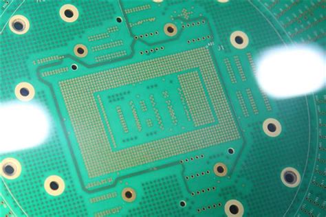
Layers of a PCB: A Comprehensive Guide
Printed Circuit Boards (PCBs) are the backbone of modern electronics, serving as the foundation upon which electronic components are mounted and interconnected. PCBs are used in a wide range of applications, from simple consumer electronics to complex industrial machinery and aerospace systems. The design and structure of a PCB are critical to its functionality, and one of the most important aspects of PCB design is the arrangement and use of its layers. This article will explore the various layers of a PCB, their functions, and how they contribute to the overall performance of the board.
1. Introduction to PCB Layers
A PCB is essentially a multi-layered sandwich of conductive and insulating materials. The layers are stacked together and bonded to form a single, cohesive unit. The number of layers in a PCB can vary depending on the complexity of the circuit and the specific requirements of the application. Simple PCBs may have only one or two layers, while more complex boards can have dozens of layers.
The layers of a PCB can be broadly categorized into two types: conductive layers and non-conductive layers. Conductive layers are used to carry electrical signals between components, while non-conductive layers provide insulation and structural support. Each layer has a specific role to play in the overall functionality of the PCB.
2. Conductive Layers
Conductive layers are the most critical part of a PCB, as they are responsible for carrying electrical signals between components. These layers are typically made of copper, which is an excellent conductor of electricity. The conductive layers are etched to form traces, pads, and vias, which are the pathways that allow electrical current to flow through the board.
2.1 Signal Layers
Signal layers are the primary conductive layers in a PCB. They are used to route electrical signals between components. The number of signal layers in a PCB depends on the complexity of the circuit. Simple single-sided or double-sided PCBs have one or two signal layers, respectively. More complex multi-layer PCBs can have four, six, eight, or even more signal layers.
In multi-layer PCBs, signal layers are often arranged in pairs, with one layer dedicated to horizontal traces and the other to vertical traces. This arrangement helps to minimize crosstalk and interference between signals, improving the overall performance of the board.
2.2 Power and Ground Layers
Power and ground layers are specialized conductive layers that are used to distribute power and provide a reference ground for the circuit. These layers are typically placed adjacent to each other to form a power-ground plane pair. The power layer carries the voltage supply (e.g., VCC) to the components, while the ground layer provides a return path for the current.
Power and ground layers are essential for maintaining stable voltage levels and reducing noise in the circuit. They also help to minimize electromagnetic interference (EMI) by providing a low-impedance path for high-frequency currents.
2.3 Split Planes
In some PCBs, the power and ground layers may be divided into multiple sections, known as split planes. Split planes are used when different parts of the circuit require different voltage levels or when it is necessary to isolate certain sections of the circuit to prevent interference. For example, a PCB for a mixed-signal circuit (combining analog and digital components) might have separate power and ground planes for the analog and digital sections to prevent noise from the digital section from affecting the analog signals.
3. Non-Conductive Layers
Non-conductive layers, also known as dielectric layers, provide insulation between the conductive layers and give the PCB its structural integrity. These layers are typically made of materials such as FR-4, a glass-reinforced epoxy laminate, which is the most common substrate material used in PCBs.
3.1 Substrate Layer
The substrate layer is the core material of the PCB, providing the base upon which the conductive layers are built. The substrate is typically made of a rigid material like FR-4, but flexible PCBs may use materials like polyimide. The substrate layer is non-conductive and provides mechanical support to the board, ensuring that it can withstand the physical stresses of assembly and operation.
3.2 Prepreg Layer
Prepreg (pre-impregnated) layers are used to bond the conductive layers together in a multi-layer PCB. Prepreg is a fiberglass material that is pre-impregnated with resin. When heated and pressed during the PCB manufacturing process, the resin flows and bonds the layers together, forming a solid, cohesive structure. Prepreg layers also provide additional insulation between the conductive layers.
3.3 Solder Mask Layer
The solder mask layer is a thin, protective coating applied over the conductive layers of the PCB. Its primary purpose is to prevent solder from bridging between conductive traces during the soldering process, which could cause short circuits. The solder mask also protects the copper traces from oxidation and environmental damage.
The solder mask is typically green, but it can also be found in other colors, such as red, blue, or black, depending on the design requirements. Openings in the solder mask, known as solder pads, are left exposed to allow components to be soldered to the board.
3.4 Silkscreen Layer
The silkscreen layer is the topmost layer of the PCB and is used to print text, symbols, and other markings on the board. These markings provide important information, such as component identifiers, polarity indicators, and reference designators, which help during the assembly and debugging process. The silkscreen layer is typically white, but other colors can be used if necessary.
4. Specialized Layers
In addition to the standard conductive and non-conductive layers, some PCBs may include specialized layers to meet specific design requirements. These layers are not found in all PCBs but are used in more advanced or specialized applications.
4.1 Impedance Control Layers
Impedance control layers are used in high-speed PCB designs where signal integrity is critical. These layers are designed to maintain a consistent impedance along the signal traces, which is essential for preventing signal reflections and ensuring reliable data transmission. Impedance control is achieved by carefully selecting the thickness and dielectric constant of the substrate and prepreg layers, as well as the width and spacing of the traces.
4.2 EMI Shielding Layers
EMI (electromagnetic interference) shielding layers are used to protect sensitive circuits from external electromagnetic interference and to prevent the PCB from emitting interference that could affect other devices. EMI shielding can be achieved by adding a conductive layer, such as a copper plane, around the perimeter of the PCB or by using specialized materials that absorb or reflect electromagnetic waves.
4.3 Thermal Management Layers
Thermal management layers are used in PCBs that generate significant amounts of heat, such as those used in power electronics or high-performance computing. These layers are designed to dissipate heat away from critical components, preventing overheating and ensuring reliable operation. Thermal management layers may include metal cores, heat sinks, or thermally conductive materials integrated into the PCB.
5. Layer Stackup and Design Considerations
The arrangement of layers in a PCB, known as the layer stackup, is a critical aspect of PCB design. The stackup determines the electrical and mechanical properties of the board, including signal integrity, power distribution, and thermal performance. When designing a PCB, engineers must carefully consider the number and arrangement of layers to meet the specific requirements of the application.
5.1 Symmetrical Stackup
A symmetrical stackup is one in which the layers are arranged symmetrically around the center of the PCB. This arrangement helps to prevent warping and ensures even distribution of mechanical stress during the manufacturing process. Symmetrical stackups are commonly used in multi-layer PCBs to maintain balance and stability.
5.2 Signal Integrity
Signal integrity is a key consideration in PCB design, especially for high-speed circuits. The placement of signal layers relative to power and ground layers can have a significant impact on signal quality. For example, placing a signal layer between two ground layers can help to reduce crosstalk and electromagnetic interference, improving signal integrity.
5.3 Power Distribution
The arrangement of power and ground layers is also critical for ensuring stable power distribution across the PCB. Placing power and ground layers close together reduces the impedance of the power distribution network, minimizing voltage drops and ensuring that all components receive a stable supply voltage.
5.4 Thermal Management
Thermal management is another important consideration in PCB design, particularly for high-power applications. The placement of thermal management layers, such as metal cores or heat sinks, must be carefully planned to ensure effective heat dissipation and prevent overheating of critical components.
6. Conclusion
The layers of a PCB are the building blocks that determine its functionality, performance, and reliability. From the conductive signal layers that carry electrical signals to the non-conductive substrate and solder mask layers that provide insulation and protection, each layer plays a vital role in the overall operation of the board. Understanding the different types of layers and their functions is essential for designing PCBs that meet the specific requirements of modern electronic applications.
As technology continues to advance, the complexity of PCBs is likely to increase, with more layers and specialized materials being used to meet the demands of high-speed, high-power, and high-density circuits. By carefully considering the arrangement and design of PCB layers, engineers can create boards that deliver optimal performance, reliability, and longevity.


