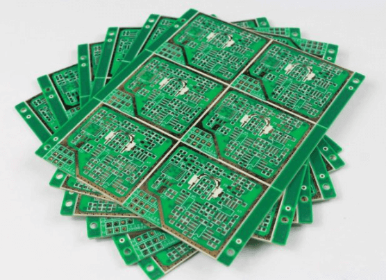
Leading Innovations in Copper Clad Board Manufacturing
Key Takeaways
The copper clad board manufacturing landscape has been significantly transformed by recent innovations that enhance both quality and efficiency in the production of Printed Circuit Boards (PCBs). As industry leaders embrace advanced materials and techniques, the importance of pcb assembly processes has become more pronounced. These innovations allow for more precision in pcba, reducing waste and lowering production costs, which is crucial in meeting the demands of modern electronics. The integration of automated systems has also streamlined workflows, enabling manufacturers to maintain high standards while increasing output. Additionally, environmentally friendly practices are gaining traction, focusing on sustainable sourcing of raw materials and minimizing the ecological footprint during production. As the sector evolves, collaboration with technology partners will likely play a key role in driving further developments in copper clad board technology, ensuring that future PCBs continue to meet the rigorous standards required by various applications across industries.
Introduction to Copper Clad Board Manufacturing
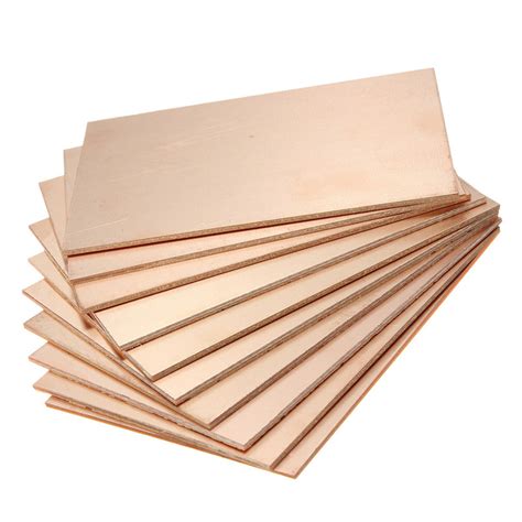
Copper clad boards are fundamental components in the printed circuit board (PCB) industry, serving as the foundation for electrical connections and providing essential structural integrity. The manufacturing of these boards has evolved significantly over the years, incorporating advanced techniques that cater to the growing demands of modern electronics. These innovations not only enhance the quality of PCBA (printed circuit board assembly) processes but also improve overall efficiency in production.
In the early days, copper clad boards were predominantly produced using manual methods that limited precision and scalability. However, today’s manufacturing landscape is characterized by automation and sophisticated processes, which deliver superior consistency and quality. For instance, techniques such as laser etching and hot-press lamination have revolutionized how layers of copper are applied to substrate materials, allowing for more intricate designs and better performance in various applications.
“Staying abreast of technological advancements is crucial for manufacturers aiming to compete in today’s fast-paced market.”
Furthermore, as we look towards the future, it’s essential to recognize that continuous improvements in material science will lead to even more robust and efficient copper clad board solutions. As electronic devices become increasingly complex—demanding greater reliability and performance from their components—the focus on innovating PCBA processes will ensure that manufacturers can meet these challenges head-on while adhering to industry standards. This ongoing evolution in copper clad board manufacturing plays a pivotal role in shaping the next generation of electronic devices.
Key Innovations Shaping the Future of PCBs
The landscape of PCB (Printed Circuit Board) manufacturing has been significantly transformed by several key innovations that are not only enhancing the quality of pcb assembly but also improving efficiency within the industry. One notable advancement is the implementation of high-frequency materials, which allow for better signal integrity in devices that demand robust performance. Furthermore, developments in additive manufacturing techniques have made it possible to produce complex geometries with reduced waste, directly benefiting the cost-effectiveness of productions such as pcba.
Another groundbreaking innovation is the increasing integration of smart technologies and automated processes, which facilitate real-time monitoring and quality assurance throughout the manufacturing lifecycle. Automation reduces human error and accelerates production times, paving the way for a more agile approach to copper clad board production. Coupled with these transformations is the rise of environmentally friendly manufacturing methods that not only comply with global regulations but also focus on sustainability—a concern that is rapidly gaining traction among consumers.
To summarize some of these innovations visually, consider the following table:
| Innovation | Description | Impact on PCB Manufacturing |
|---|---|---|
| High-Frequency Materials | Enhance signal integrity | Improved performance in devices |
| Additive Manufacturing | Allows for complex geometries | Reduced waste and cost-effectiveness |
| Smart Technologies | Real-time monitoring and quality assurance | Increased efficiency |
| Environmentally Friendly | Sustainable production methods | Compliance with regulations |
As we move forward, these innovations serve as a cornerstone for future advancements in pcb assembly processes, leading to enhanced performance levels in electronic devices while maintaining environmental responsibility. The continuous evolution in this field underscores not just technological prowess but also reflects an industry-wide commitment to higher standards and better solutions for modern consumer demands.
Industry Leaders in Copper Clad Board Technology
The landscape of copper clad board manufacturing is significantly influenced by a number of industry leaders known for their innovative practices and commitment to quality. These manufacturers employ various advanced techniques to enhance not only the durability but also the functionality of PCB technologies. Companies such as Rogers Corporation, Hitachi Chemical, and Isola Group are at the forefront, pushing the boundaries of what is possible in pcb assembly and contributing to the evolution of PCBA processes. Their focus on developing high-performance materials allows for lighter, thinner, and more efficient boards, which are essential in meeting the demands of modern electronic devices. By integrating cutting-edge technologies such as automated production lines and advanced plating methods, these leaders are able to produce boards that minimize signal loss, manage thermal dynamics effectively, and support intricate patterns necessary for today’s micro-electronics. This ongoing pursuit not only augments quality but also elevates overall efficiency in manufacturing cycles, thereby setting a benchmark for competitors within the industry. As they continue to innovate, these leaders pave the way toward a future where copper clad boards will be even more integral to advancing electronic applications across various sectors.
Advanced Techniques in Manufacturing Processes
In recent years, the copper clad board manufacturing industry has witnessed significant advancements in production techniques, leading to enhanced quality and efficiency in pcb assembly and pcba processes. One notable innovation is the implementation of precision laser cutting technology, which allows for intricate designs and improves the overall accuracy of board fabrication. This method not only minimizes waste but also enables manufacturers to create more complex circuits that meet the growing demands of modern electronics.
Additionally, techniques such as automated optical inspection (AOI) are becoming increasingly prevalent in ensuring the quality of the output. AOI systems significantly reduce error rates during production by using advanced imaging systems to catch faults early in the process, thus providing a higher standard of reliability for pcb assembly. Coupled with robotic assembly solutions, these methodologies streamline operations and enhance productivity.
Moreover, advancements in material science have introduced new copper clad substrates that offer better electrical performance and thermal management. As manufacturers adopt these innovative materials, the efficiency of pcba processes is heightened, supporting a broader range of applications from consumer electronics to aerospace.
Overall, these cutting-edge techniques are setting new benchmarks within the industry. They not only improve operational efficiencies but also promote sustainability by reducing material waste and energy consumption during production cycles. As manufacturing continues to evolve with these advancements, the landscape of copper clad board technology is poised for considerable growth.
Enhancing Quality and Efficiency in Electronics
In the realm of electronics, the demand for high-performance PCB assembly is driving innovations in manufacturing processes, particularly in the production of copper clad boards. These advancements focus on enhancing both quality and efficiency, ensuring that the final products meet stringent performance standards. One significant innovation is the development of advanced materials that improve conductivity and thermal management. By utilizing improved copper clad boards, manufacturers can produce more reliable circuits, thereby increasing the overall effectiveness of pcba solutions.
Moreover, incorporating state-of-the-art technologies such as automated testing and precision cutting allows for a reduction in manufacturing errors, leading to a decrease in waste and production time. Additionally, this helps streamline supply chains by enabling faster turnaround times while maintaining high product quality. As manufacturers continually refine their processes in copper clad board production, they are also observing notable improvements in scalability and customization options for their pcb assembly needs. This results in greater flexibility for clients requiring tailored solutions without sacrificing efficiency or cost-effectiveness. Thus, these enhancements not only support industry growth but also play a crucial role in meeting evolving consumer demands in the electronics sector.
Environmental Considerations in Copper Clad Board Production
The manufacturing of copper clad boards has begun to embrace a more environmentally conscious approach, responding to the growing demand for sustainable practices in the electronics industry. As the production of PCBs (Printed Circuit Boards) becomes increasingly scrutinized, manufacturers are implementing innovative strategies aimed at reducing waste and energy consumption. One prominent method involves optimizing the pcb assembly process to minimize material usage while maintaining the integrity and performance of the final product. Furthermore, some leading companies are exploring alternatives to traditional chemicals used in etching and laminating processes, favoring eco-friendly solutions that lessen harmful environmental impacts. Investing in pcba technology that emphasizes recyclability is also gaining traction, encouraging a circular economy within this sector. As these developments unfold, it’s clear that an environmentally sustainable mindset not only enhances public perception but can also lead to long-term cost savings and increased efficiency for manufacturers dedicated to high-quality copper clad boards. These advancements hold great promise for future production methods while ensuring that environmental responsibility remains at the forefront of industry innovation.
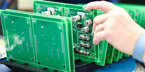
The Role of Automation in Modern PCB Manufacturing
Automation has become a pivotal force in enhancing the efficiency and precision of PCB assembly processes. The integration of advanced technologies, such as robotics and artificial intelligence, allows manufacturers to optimize every aspect of pcba production. Automation facilitates rapid prototyping, where components can be assembled at an unprecedented speed while maintaining high-quality standards. This precision is essential in copper clad board manufacturing, where even the slightest deviation can lead to significant defects in functionality. Additionally, automation reduces the reliance on manual labor, thereby minimizing human error and enabling consistent quality across batches. Manufacturers can leverage automated systems to monitor multiple stages of production in real time, ensuring that any issues are promptly identified and rectified. As copper clad boards serve as a backbone for various electronic devices, innovations driven by automation are crucial for meeting the growing demands of the electronics industry and ensuring that products remain competitive in a fast-evolving market. The future will likely see further advancements in automated technologies, enhancing not only the speed but also the sustainability of pcba processes while supporting manufacturers in achieving their environmental goals.
Future Trends and Predictions for the Industry
As the landscape of copper clad board manufacturing evolves, several emerging trends are poised to reshape the industry. One significant trend is the increasing integration of smart manufacturing technologies. These advancements enable more precise control over the production process, ensuring higher quality in pcb assembly and ultimately enhancing the performance of pcba. Furthermore, companies are investing in sustainable practices—from utilizing eco-friendly materials to optimizing supply chains—that align with global environmental goals. This shift emphasizes a relevant dichotomy in production: while efficiency is paramount, there is also a strong focus on minimizing environmental impact. Additionally, the rise of flexible PCBs reflects growing demands for lightweight and adaptable electronics, particularly in sectors such as consumer electronics and automotive. As manufacturers incorporate innovative designs and materials, they will likely see an increase in market competitiveness and consumer satisfaction. The future also hints at advancements in automation techniques that can streamline assembly processes further, resulting in shorter lead times and reduced costs for pcb assembly services across various industries. Ultimately, these trends indicate a promising trajectory for copper clad board manufacturers as they adapt to changing consumer needs and technological advancements in the electronics sector.
Conclusion
In conclusion, copper clad boards play a crucial role in the performance of printed circuit boards (PCBs), and the advancements in copper clad board manufacturing are paving the way for superior pcb assembly processes. As manufacturers adopt innovative techniques that enhance the properties of pcb assemblies, they also improve overall efficiency and durability. The integration of automation and modern technologies ensures that production is not only faster but also more reliable, resulting in a significant reduction in defects. This focus on quality translates into better-performing electronics, ultimately benefiting industries spanning from consumer electronics to aerospace. As we look toward the future, it is evident that continued investment in research and development will drive further innovations within copper clad board technology. Thus, by embracing these advancements, manufacturers can meet evolving industry demands and contribute significantly to the growth of the pcba landscape.
FAQs
What is a copper clad board?
A copper clad board, commonly used in PCB assembly, is a substrate coated with a layer of copper on one or both sides, providing the necessary conductive paths for electronic circuits.
What are the main applications of copper clad boards?
Copper clad boards are essential in various applications, including consumer electronics, telecommunications, and automotive industries, where reliable pcba is crucial for functioning devices.
How does the manufacturing process of copper clad boards affect their quality?
The manufacturing process involves intricate techniques that directly influence the quality of the final product. Employing advanced technologies ensures that the copper layers are uniformly applied, resulting in higher efficiency and reliability in pcb assembly.
What role do industry leaders play in advancing copper clad board technology?
Industry leaders drive innovation by investing in research and development. Their expertise contributes to creating more efficient processes and materials, which ultimately enhance the performance and durability of pcba.
How can I learn more about PCB assembly services?
To explore comprehensive solutions related to pcb assembly, please click here. Our team provides insights into advanced techniques and services available to meet your needs.