Mastering Complex PCB Assembly: Your Guide to Precision and Efficiency
Key Takeaways
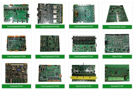
Mastering PCB assembly is essential for both professionals and enthusiasts in the field of electronics. A thorough understanding of the key components involved in the process, such as various types of electronic components, substrate materials, and soldering techniques, is vital for achieving success. In complex PCB assembly (PCBA), precision is paramount; every connection must be executed flawlessly to ensure reliable operation. Implementing advanced techniques such as automated placement and soldering can significantly enhance both efficiency and accuracy, leading to higher quality products. Moreover, streamlining the assembly process by adopting robust practices fosters reduced lead times and costs.
However, assembling complex PCBs is not without its challenges. Common issues like misalignment of components or solder defects can arise, but by understanding these pitfalls and knowing effective solutions—such as employing more refined inspection methods or utilizing improved software tools—engineers can navigate these difficulties with greater ease. To ensure a successful PCBA, it is also critical to invest in appropriate tools and technologies that facilitate effective project management and execution. Emphasizing thorough testing and robust quality assurance measures during the assembly phase ensures that every product meets stringent industry standards. As technology evolves, staying informed about future trends in complex PCB design will provide engineers with innovative ideas to maintain competitiveness in a rapidly changing marketplace.
Understanding the Basics of PCB Assembly
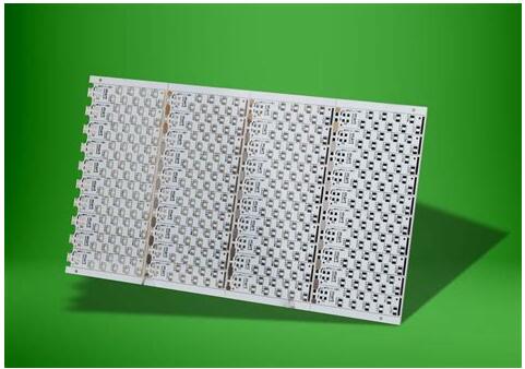
To grasp the fundamentals of PCB assembly, or PCBA, it’s essential to understand that this process involves connecting various components onto a printed circuit board (PCB) to form a complete electronic circuit. The complexity of the assembly can vary significantly based on the design specifications and components used. It’s crucial to identify the different types of components such as resistors, capacitors, and integrated circuits, as well as how they interact within the PCB layout. The assembly process can be approached using methodologies such as through-hole or surface mount technology, each offering distinct advantages depending on the project’s requirements.
The quality and precision in PCB assembly are paramount, particularly for complex designs that incorporate densely packed components. Maintaining high standards in soldering techniques and component placement can significantly reduce common errors. Therefore, having a thorough understanding of the PCB layout, including traces and pads, contributes to minimizing potential issues during assembly. As noted by industry experts:
“Attention to detail in the early stages leads to smoother production later on.”
This principle emphasizes that an accurate understanding of both design and assembly processes ensures higher efficiency and reliability.
Moreover, familiarity with tools such as reflow ovens for surface mount soldering or wave soldering machines for through-hole parts is beneficial. Adequate training in using these technologies will improve not only individual skills but also team workflows. With technological advancements continually shaping complex PCB assembly, staying updated on best practices is essential for engineers and hobbyists looking to excel in this evolving field.
Key Components of Complex PCB Design
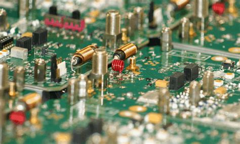
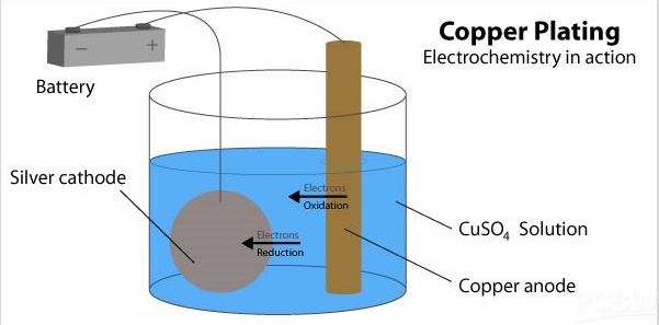
In the realm of pcb assembly, understanding the key components that contribute to effective pcba is essential for both novice and experienced designers. The first crucial element is the substrate material, which serves as the foundation for all other components. It defines how well electrical signals can perform and affects the overall durability of the assembled product. Next, we have conductive pathways—usually made from copper—which facilitate the flow of electricity across different parts of the board. Designers must carefully consider their layout to minimize signal loss and interference.
Another significant aspect is the use of components like resistors, capacitors, and integrated circuits. Each component must be selected based on specific electrical characteristics to ensure optimal performance in varying conditions. In modern designs, multilayer PCBs are commonly utilized, allowing for more complex circuits within a compact space while ensuring thermal management and signal integrity are maintained.
Furthermore, proper placement and orientation of these components during pcb assembly are vital for ease of manufacture and functionality. Factors such as thermal expansion, environment, and electrical performance all play a role in component selection. Finally, innovative technologies such as automated assembly lines have revolutionized how these components come together, enhancing efficiency while maintaining high standards for quality in the finished product.
In summary, each element plays a crucial role in ensuring that complex pcb assembly meets its design specifications without compromising on quality or efficiency. Understanding these components will empower developers to navigate their projects with greater confidence and precision.
Techniques for Enhancing Precision in Assembly
Achieving high levels of precision in pcb assembly is critical for the reliability and functionality of printed circuit boards (PCBs). One effective technique is the use of automated assembly equipment, which significantly minimizes human error and ensures consistent placement of components. This equipment includes pick-and-place machines that handle components with remarkable accuracy, reducing misalignment and enhancing overall quality in the pcba process.
Moreover, implementing advanced soldering techniques such as reflow soldering or wave soldering can further improve adhesion and reduce defects. Careful control of temperature and timing during these processes ensures that solder joints meet the necessary standards, which is vital for the durability of the PCB. Additionally, employing high-resolution optical inspection systems during assembly allows for real-time monitoring. This tactic helps identify defects early in the process, enabling quick adjustments to maintain precision levels.
Another aspect to consider is component selection; choosing components that are compatible with automated assembly methods can greatly improve precision. A table summarizing recommended practices for component selection might include:
| Component Type | Recommendation | Reason |
|---|---|---|
| SMT Components | Use standard sizes | Ensures compatibility with automated machines |
| Via Design | Opt for through-hole where possible | Easier handling during assembly |
| Pad Design | Ensure proper pad widths | Enhances solder joint reliability |
To sum up, integrating automated technologies, refining soldering techniques, and making informed component choices are fundamental to achieving optimal pcb assembly precision. Through these methods, engineers can ensure that their projects not only meet but exceed industry standards, ultimately leading to successful outcomes in their endeavors.
Streamlining the Assembly Process for Efficiency
Efficient PCB assembly is crucial for the successful deployment of electronic devices, especially when working with complex designs. One effective approach to streamline the assembly process is to implement a modular design strategy. By breaking down the PCBA into smaller, manageable sections, engineers can focus on optimizing each part before integrating them into a complete system. This not only accelerates the assembly timeline but also allows for easier identification of issues during the build process.
Another key technique is to leverage advanced automation tools. Utilizing robotic arms and automated soldering techniques can significantly reduce human error and increase production speeds. Additionally, employing smart manufacturing practices enables real-time monitoring of assembly lines, ensuring any deviations from standard procedures are promptly addressed.
For engineers and hobbyists alike, adopting a lean manufacturing mindset can yield substantial improvements in efficiency. This involves minimizing waste—whether in materials or time—by continuously assessing workflow and identifying bottlenecks. Implementing approaches such as Kanban systems can help track progress and manage resources more effectively.
Moreover, fostering collaboration between design and manufacturing teams will enhance communication and ensure that all aspects of PCB assembly are aligned with project goals. By prioritizing both precision and efficiency through these strategies, individuals involved in PCBA can deliver high-quality products that meet both functional requirements and market demands.
Common Challenges in Complex PCB Assembly and Solutions
In the world of PCB assembly, various challenges can arise that may impede the successful execution of projects. One common issue is the complexity of PCBA design itself, which often features densely packed components and intricate layouts. This can lead to difficulties in soldering processes, resulting in cold joints or bridging between pads. To address these issues, adopting advanced soldering techniques and maintaining optimal temperature profiles during soldering can significantly improve the integrity of the connections.
Another challenge involves maintaining precision in component placement, particularly with smaller surface-mounted devices (SMDs) that require meticulous handling. Utilizing automated pick-and-place machinery equipped with advanced vision systems can enhance positioning accuracy while reducing manual errors. Furthermore, ensuring that all components conform to strict tolerances can also be challenging during assembly. Implementing precise alignment fixtures and leveraging computer-aided design (CAD) software for verification before assembly can mitigate potential discrepancies.
Additionally, duplicating quality across multiple PCBA iterations poses its own challenges, particularly when scaling production. Keeping a thorough inventory management system and standardizing operating procedures can help ensure consistency across batches while maintaining high levels of efficiency. By proactively addressing these common challenges with targeted solutions, engineers and hobbyists alike can greatly enhance both the precision and efficiency of their PCB assembly projects, ultimately leading to superior outcomes in their electronic designs.
Tools and Technologies for Successful PCB Projects
In the realm of pcb assembly, leveraging the right tools and technologies is crucial for achieving optimal results. A variety of software programs aid in the design and simulation of pcb designs, enabling engineers to visualize their layouts before moving into production. Programs like Altium Designer or KiCad provide comprehensive platforms for designing intricate printed circuit boards (PCBs), making it easier to anticipate potential issues during the assembly phase.
Moreover, automated assembly machines significantly enhance efficiency in pcba processes. These machines, which include pick-and-place equipment, are capable of placing components with remarkable precision, reducing human error and increasing throughput. Soldering techniques, such as reflow soldering or wave soldering, are essential technologies that ensure reliable connections between components on the PCB, further enhancing reliability and performance.
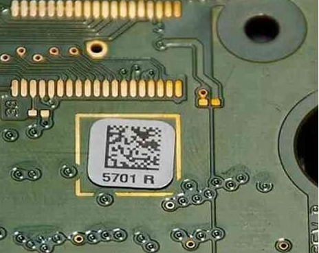
Additionally, the integration of advanced technologies like surface mount technology (SMT) and through-hole technology allows for more compact designs while maintaining effective signal integrity. These methods work hand-in-hand with various inspection tools like Automated Optical Inspection (AOI), ensuring that every assembled board meets stringent quality standards.
By utilizing these tools and technologies effectively in pcb assembly, both engineers and hobbyists can streamline their workflows, minimize errors, and elevate the quality of their PCBs to meet demanding project specifications while staying competitive in an ever-evolving industry landscape.
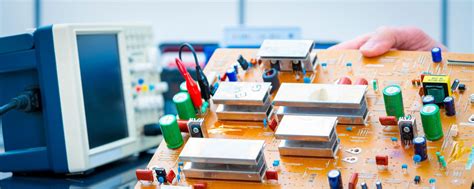
Testing and Quality Assurance in PCB Assembly
Ensuring the quality and functionality of PCB assembly is paramount for delivering reliable electronic products. The testing process in PCBA involves several methodologies designed to catch defects early and validate that each pcb assembly meets its specified requirements. One common method employed is the Automated Optical Inspection (AOI), which uses sophisticated imaging technology to examine the components and solder joints for precision. Following AOI, functional testing simulates the operating conditions of the assembled boards, ensuring that all circuits function correctly. It is essential for identifying issues that visual inspections might overlook.
Another aspect of quality assurance involves in-circuit testing (ICT), which assesses each component’s integrity by creating a reliable connection through test probes and verifying electrical characteristics against expected values. This method is particularly effective in complex pcb assemblies, where multiple layers can obscure faults. Additionally, reliability tests like thermal cycling and humidity exposure help determine how well the assembly holds up under varying environmental conditions.
Implementing a rigorous quality assurance protocol not only increases the longevity and performance of electronic devices but also reduces scrap and rework costs associated with defective PCBA. By adopting these testing strategies, engineers can ensure that their complex PCB assembly processes yield products that not only meet but exceed expectations in precision and efficiency.
Future Trends in Complex PCB Design and Assembly
As technology continues to evolve, complex PCB assembly (PCBA) practices are expected to undergo significant transformations that will enhance both design and production processes. One of the most notable trends is the increasing integration of automation and artificial intelligence into the assembly lines, which promises to improve precision and reduce the overall time required for production. This shift toward automation is particularly beneficial for handling intricate designs, allowing engineers to maintain high standards of quality while streamlining workflows.
Additionally, the demand for miniaturization in electronic devices has prompted a push for more compact PCB designs. This trend not only necessitates advancements in assembly techniques but also requires innovative approaches to material selection. Utilizing advanced substrates and components will enable manufacturers to create smaller assemblies without compromising performance.
Furthermore, sustainability is becoming a key consideration in complex PCB assembly practices. Manufacturers are now focusing on eco-friendly materials and processes that reduce waste and energy consumption during production. This commitment aligns with global efforts toward greener technology and reflects consumers’ growing preference for environmentally responsible products.
Lastly, the increasing interconnectedness of devices through the Internet of Things (IoT) emphasizes the importance of robust PCBA designs that can withstand diverse operating conditions. Emerging design methodologies, such as modularity and flexibility, will be essential in developing PCBs that can adapt to various applications while ensuring reliability across different scenarios.
In conclusion, the future of complex PCB design and assembly looks promising as these trends converge to create higher efficiency and greater precision within the industry. As engineers continue to refine their approaches with these developments, we can expect remarkable advancements in both functionally complex circuitry and overall product performance.
Conclusion
In this guide, we have delved into the intricacies of complex PCB assembly and highlighted the paramount importance of precision and efficiency in PCBA. Mastering the nuances of pcb assembly not only enhances the overall quality of electronic devices but also significantly reduces production time and costs. Each key component in PCB design plays a critical role; hence understanding these elements is essential for anyone involved in this field, from engineers to hobbyists. Moreover, by implementing advanced techniques for enhancing precision, such as adopting automated assembly processes or utilizing sophisticated software tools, one can further streamline their projects. Recognizing and addressing common challenges is equally important to ensure that your PCBA projects adhere to industry standards. As we look towards the future, keeping abreast of emerging trends and technologies will undoubtedly shape the next generation of complex PCB assembly, driving innovation and paving the way for even greater achievements in this dynamic field.
FAQs
What is complex PCB assembly?
Complex PCB assembly refers to the intricate process of assembling printed circuit boards (PCBs) that involve multiple layers, components, and advanced features. This type of pcba demands a high level of precision and often incorporates surface mount technology (SMT) and through-hole components to create a fully functional electronic assembly.
What techniques can enhance precision in PCB assembly?
To enhance precision in PCBA, techniques such as using advanced soldering methods, implementing automated placement systems, and conducting regular training sessions for staff can be highly effective. Additionally, accurate stencil printing and the use of inspection systems can significantly improve the overall quality.
How can I streamline the PCB assembly process for efficiency?
Streamlining the PCB assembly process can be achieved by optimizing the workflow, utilizing modular layouts for tools and machines, and adopting lean manufacturing principles. Investing in modern machinery such as pick-and-place machines can also reduce cycle times while ensuring consistent quality.
What are common challenges faced in complex PCB assembly?
Some common challenges in pcba include managing component obsolescence, maintaining alignment during multilayer assemblies, and addressing thermal issues caused by densely packed components. Proactive planning, rigorous testing protocols, and keeping abreast of industry changes can help mitigate these challenges.
How important is testing and quality assurance in PCB assembly?
Testing and quality assurance are critical components of any PCBA project. They ensure that the assembled boards meet industry standards and function as intended. This includes visual inspections, automated optical inspection (AOI), functional testing, and burn-in tests to catch defects early.