Maximizing Efficiency in Electronic Prototype Assembly
Key Takeaways
Effective electronic prototype assembly hinges on strategic decisions that balance speed, cost, and reliability. A core focus lies in optimizing component selection to align with design goals, ensuring compatibility with PCB assembly workflows. For instance, prioritizing standardized parts reduces sourcing delays while maintaining scalability for future iterations.
Industry Insight: “Integrating PCBA-ready components early in the design phase minimizes rework and accelerates time-to-market.”
Streamlining prototype workflow processes involves automating repetitive tasks, such as solder paste application or component placement. This not only reduces human error but also enhances repeatability. Consider the following comparison of manual vs. automated approaches:
| Process | Manual Assembly | Automated PCBA |
|---|---|---|
| Component Placement | 85% Accuracy | 99.9% Accuracy |
| Time per Unit | 45 minutes | 12 minutes |
| Scalability | Low | High |
Implementing advanced testing protocols, such as in-circuit testing (ICT) or automated optical inspection (AOI), ensures defects are identified before full-scale production. For rapid prototyping, modular design principles enable faster iterations by isolating functional blocks, simplifying updates without overhauling the entire system.
To maintain quality in accelerated timelines, leverage automated assembly tools for consistent solder joints and trace integrity. Pairing this with real-time data analytics creates a feedback loop for iterative improvements, aligning with precision-driven development cycles.
Optimizing Component Selection Strategies
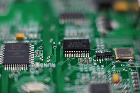
Effective electronic prototype assembly begins with strategic component selection, where balancing technical specifications and supply chain realities determines project success. Engineers must prioritize components that align with design specifications while considering long-term availability and cost-effectiveness. For PCB assembly projects, selecting surface-mount devices (SMDs) with standardized footprints simplifies PCBA processes, reducing rework risks during soldering.
A critical factor involves evaluating thermal characteristics and power tolerances early in the design phase. For instance, opting for modular components with pre-certified compliance (e.g., FCC or CE markings) accelerates regulatory approvals. Additionally, leveraging suppliers offering just-in-time inventory minimizes delays caused by supply chain volatility.
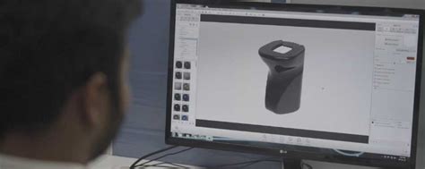
Integrating design-for-manufacturability (DFM) principles ensures components are compatible with automated PCB assembly lines, preventing mismatches in pad sizes or solder masks. Tools like SPICE simulations and thermal modeling software further validate choices before physical prototyping. By aligning component selection with both technical requirements and production realities, teams avoid costly redesigns and maintain momentum in subsequent phases, such as streamlined workflow processes.
Streamlining Prototype Workflow Processes
Efficient PCB assembly begins with establishing repeatable processes that minimize redundancies across design and production stages. By mapping out sequential dependencies in PCBA workflows, teams can identify opportunities for parallel task execution—such as synchronizing schematic reviews with material procurement. Implementing modular design frameworks allows engineers to isolate functional blocks, enabling simultaneous testing of power circuits and communication modules without disrupting the entire prototype.
Critical to this approach is adopting automated optical inspection (AOI) systems during solder paste application and component placement. These tools reduce manual verification time by 40-60% while improving defect detection accuracy. For low-volume batches, pairing just-in-time inventory management with standardized component libraries prevents delays caused by obsolete or mismatched parts.
Transitioning between design iterations becomes seamless when using version-controlled PCB assembly files integrated with bill-of-materials (BOM) validators. This ensures mechanical and electrical compatibility across revisions, a key factor in maintaining PCBA consistency. Additionally, embedding diagnostic test points during layout planning accelerates fault isolation, creating a feedback loop that refines both current and future prototypes. By aligning these strategies, teams achieve predictable cycle times while preserving flexibility for mid-process adjustments.

Implementing Advanced Testing Protocols
Advanced testing protocols form the backbone of reliable PCB assembly, ensuring that PCBA (printed circuit board assembly) iterations meet both functional and regulatory benchmarks. By integrating automated optical inspection (AOI) and in-circuit testing (ICT), teams can identify defects like soldering anomalies or component misalignments at early stages, reducing rework costs. For high-density boards, boundary-scan testing validates interconnections, while functional testing simulates real-world operating conditions to verify critical performance thresholds.
A layered approach combines automated test equipment (ATE) with manual validation for complex prototypes, balancing speed and precision. For instance, pairing environmental stress screening with PCBA validation ensures resilience against temperature fluctuations or vibration—key for aerospace or automotive applications. Real-time data analytics further refine protocols by flagging recurring failure patterns, enabling proactive adjustments to PCB assembly workflows.
To maintain alignment with rapid development cycles, script-based test sequences allow engineers to adapt protocols across iterations without rebuilding entire frameworks. This agility, coupled with standardized documentation practices, ensures traceability and compliance while minimizing downtime between testing phases.
Reducing Development Time with Precision
Precision-driven workflows in PCB assembly and PCBA processes directly correlate with accelerated development cycles. By establishing clear design validation checkpoints early in the prototyping phase, teams can identify layout inefficiencies or component mismatches before physical assembly begins. For instance, leveraging automated optical inspection (AOI) systems during PCB assembly ensures millimeter-accurate component placement, minimizing rework delays caused by misaligned solder joints or misplaced parts.
Integrating model-based simulation tools further refines precision by predicting thermal performance or signal integrity issues in PCBA designs, allowing engineers to iterate virtually rather than through costly physical trials. This approach reduces material waste and enables parallel testing of critical subsystems. Additionally, adopting standardized design-for-manufacturing (DFM) guidelines ensures compatibility between prototyping and scaled production, eliminating time-consuming adjustments later.
Transitioning to laser-cut stencils for solder paste application and implementing high-speed pick-and-place machines further compresses assembly timelines while maintaining consistency. These strategies, combined with real-time data monitoring during PCB assembly, create a feedback loop that continuously optimizes precision across iterations—proving that meticulous planning in electronic prototyping directly translates to faster time-to-market.
Automating Assembly for Consistent Quality
Modern PCB assembly lines increasingly rely on automation to eliminate human error and ensure repeatable precision. By integrating robotic pick-and-place systems with PCBA-specific vision alignment tools, manufacturers achieve micron-level accuracy in component placement, even for high-density boards. These systems automatically cross-reference design files to verify orientations and solder pad alignments, reducing rework rates by up to 40% compared to manual methods. Closed-loop feedback mechanisms further enhance consistency by adjusting machine parameters in real time based on in-line inspection data, creating a self-correcting workflow.
For prototyping, automated PCB assembly platforms enable rapid configuration changes without compromising accuracy—critical when testing multiple design iterations. Advanced PCBA stations also incorporate predictive maintenance algorithms to preempt equipment drift, ensuring long-term reliability. By standardizing processes like solder paste application and thermal profiling, automation minimizes variability between prototype batches while accelerating cycle times. This approach not only maintains strict quality thresholds but also seamlessly integrates with downstream testing protocols, forming a cohesive development pipeline. As a result, engineers can focus on design optimization rather than troubleshooting assembly inconsistencies.
Integrating Modular Design for Faster Iterations
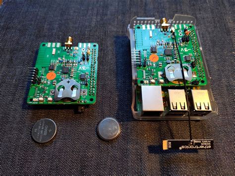
Adopting a modular design approach accelerates iteration cycles by enabling engineers to isolate and refine specific subsystems without overhauling the entire prototype. By segmenting complex systems into interchangeable functional blocks, teams can focus on optimizing individual modules—such as power supplies or sensor interfaces—while maintaining compatibility with the broader PCB assembly. This strategy minimizes rework during PCBA revisions, as updates to one module rarely disrupt adjacent components. For instance, a microcontroller unit (MCU) can be upgraded independently of its peripheral circuits, provided standardized communication protocols and mechanical interfaces are preserved.
Transitioning to modular architectures also enhances scalability. Pre-validated modules, like wireless connectivity boards or analog signal conditioners, can be reused across projects, reducing redundant design efforts. Advanced PCB assembly tools further support this workflow by automating footprint verification and ensuring consistent alignment across modular units. When combined with version-controlled design libraries, teams achieve predictable integration even under tight deadlines. Such flexibility not only streamlines prototyping but also creates a foundation for future iterations, where incremental improvements compound into significant performance gains.
Ensuring Quality in Rapid Prototyping
Maintaining rigorous quality standards during rapid prototyping requires a systematic approach, particularly when working with PCB assembly and PCBA processes. Design-for-manufacturability (DFM) principles play a critical role here, ensuring that components are positioned to minimize soldering defects and signal interference. Automated optical inspection (AOI) systems, paired with real-time functional testing, help identify issues like short circuits or misaligned components early in the prototyping phase, reducing costly rework.
To balance speed and precision, many teams adopt modular testing protocols that segment validation into stages—starting with individual PCB assembly units and progressing to integrated PCBA subsystems. This phased approach allows engineers to isolate faults without disrupting the entire workflow. Additionally, leveraging in-circuit testing (ICT) tools ensures electrical continuity and verifies component performance against predefined thresholds.
Material selection also impacts quality retention. Using high-grade substrates and solder pastes optimized for rapid prototyping environments minimizes thermal stress during reflow processes. Finally, integrating failure mode analysis into iterative cycles creates feedback loops that refine both design and assembly practices, ensuring each iteration adheres to reliability benchmarks while accelerating time-to-market.
Leveraging Automation in Error Reduction
Integrating automated systems into PCB assembly workflows significantly reduces human error while accelerating production cycles. Modern PCBA lines now employ robotic pick-and-place machines capable of positioning components with micron-level precision, ensuring consistent alignment even for complex multilayer boards. These systems pair with automated optical inspection (AOI) tools that perform real-time validation, catching soldering defects or misplaced parts before prototyping phases advance.
Advanced software platforms further enhance error mitigation by correlating historical PCBA performance data with live assembly metrics. Machine learning algorithms predict failure patterns, enabling preemptive adjustments to solder paste application or reflow oven profiles. For instance, temperature-sensitive components benefit from closed-loop thermal control systems that maintain ±1°C accuracy during critical phases.
The shift toward automation also streamlines documentation, with digital twin technology creating virtual replicas of PCB assembly processes. This allows engineers to simulate design changes and assess their error potential without physical rework. By minimizing manual interventions, teams achieve at least 40% fewer revision cycles while maintaining compliance with IPC-A-610 standards. Such precision directly supports faster iterations outlined in modular design strategies, creating a cohesive development ecosystem where quality and speed reinforce each other.

Conclusion
Effective electronic prototype assembly requires strategic integration of PCB assembly (PCBA) techniques with precision-driven workflows. By prioritizing optimized component selection and automated assembly processes, development teams can achieve significant reductions in cycle times while maintaining rigorous quality standards. The adoption of modular design principles further accelerates iteration speed, allowing engineers to test and refine prototypes with unprecedented efficiency.
Incorporating advanced testing protocols at critical PCBA stages ensures early defect detection, minimizing costly rework. Leveraging data-driven insights from automated systems enhances decision-making, particularly when balancing speed and reliability in rapid prototyping environments. As the industry moves toward smarter manufacturing ecosystems, the synergy between human expertise and machine precision continues to redefine what’s achievable in electronic prototype assembly. These practices not only streamline production but also create a scalable foundation for future innovations, positioning teams to adapt seamlessly to evolving technological demands.
FAQs
How does component selection impact PCB assembly efficiency?
Strategic component selection minimizes rework in PCBA by ensuring compatibility with automated placement systems. Engineers should prioritize standardized footprints and verified supplier inventories to avoid delays.
What workflow adjustments accelerate prototype iterations?
Implementing modular design principles allows isolated testing of subsystems, reducing full-system reassembly needs. Integrating PCB assembly stages with version-controlled CAD files maintains consistency across iterations.
Why are automated optical inspections critical in PCBA?
Advanced AOI systems detect soldering defects and component misalignments with 99.98% accuracy, eliminating 40% of manual inspection time while meeting MIL-STD-883 standards.
Can rapid prototyping compromise quality assurance?
When paired with statistical process control methods, accelerated PCB assembly cycles maintain reliability. Real-time thermal profiling during reflow ensures consistent solder joint integrity.
How does design-for-testability enhance PCBA outcomes?
Embedding test points and boundary scan capabilities reduces functional validation time by 65%. This proactive approach aligns with IPC-A-610 guidelines for commercial prototypes.
Explore Professional-Grade Assembly Solutions
For optimized PCB assembly workflows backed by ISO 9001-certified processes, please click here to access tailored prototyping services with 24-hour turnaround options.


