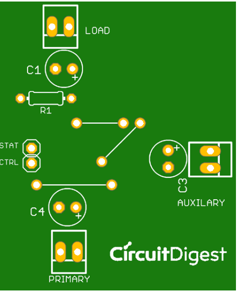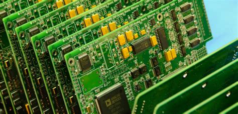
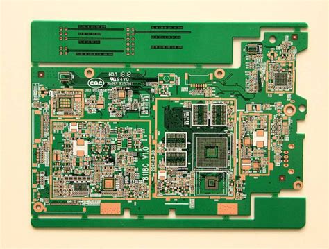
Model of pcb
Introduction To PCB Design Models
Printed Circuit Boards (PCBs) are the backbone of modern electronic devices, serving as the foundation upon which electronic components are mounted and interconnected. The design of PCBs is a meticulous process that requires a deep understanding of both the electrical and mechanical aspects of the board. To facilitate this complex task, various PCB design models have been developed, each offering unique advantages and catering to different requirements. Understanding these models is crucial for engineers and designers aiming to create efficient, reliable, and cost-effective electronic products.
One of the most fundamental models in PCB design is the single-layer PCB.
This model consists of a single layer of conductive material, typically copper, on one side of an insulating substrate. Single-layer PCBs are relatively simple and inexpensive to produce, making them ideal for low-cost, low-complexity applications such as consumer electronics and basic industrial devices. However, their simplicity also limits their functionality, as they can only accommodate a limited number of components and connections.
Transitioning from single-layer to more complex designs, the double-layer PCB model introduces a second layer of conductive material on the opposite side of the substrate.
This additional layer allows for more intricate circuit designs and greater component density. Double-layer PCBs are commonly used in more sophisticated electronic devices, including advanced consumer electronics, automotive systems, and industrial control equipment. The increased complexity of double-layer PCBs requires more advanced manufacturing techniques and design considerations, such as the use of vias to connect traces between the two layers.
As electronic devices continue to evolve, the need for even more complex PCB designs has led to the development of multi-layer PCBs.
These models consist of multiple layers of conductive material separated by insulating layers, allowing for highly complex and dense circuit designs. Multi-layer PCBs are essential for high-performance applications such as computer motherboards, telecommunications equipment, and aerospace systems. The design and manufacturing of multi-layer PCBs are significantly more challenging, requiring advanced software tools and precise fabrication processes to ensure proper alignment and connectivity between layers.
In addition to the number of layers, another critical aspect of PCB design models is the type of components used.
Surface-mount technology (SMT) and through-hole technology (THT) are the two primary methods for mounting components on a PCB. SMT involves placing components directly onto the surface of the PCB, allowing for smaller, more compact designs. This method is widely used in modern electronics due to its efficiency and ability to support high component densities. Conversely, THT involves inserting component leads through holes in the PCB and soldering them on the opposite side. While THT is less common in contemporary designs, it remains valuable for applications requiring robust mechanical connections, such as power supplies and high-stress environments.
Furthermore, the choice of materials in PCB design models plays a significant role in the board’s performance and reliability.
Common substrate materials include FR-4, a fiberglass-reinforced epoxy laminate, which offers a good balance of cost, durability, and electrical performance. For high-frequency applications, materials such as Rogers laminates provide superior signal integrity and reduced signal loss.
In conclusion, the various models of PCB design, ranging from single-layer to multi-layer configurations and incorporating different mounting technologies and materials, offer a wide array of options to meet the diverse needs of modern electronic devices. Understanding these models and their respective advantages is essential for engineers and designers to create effective and reliable PCBs that meet the demands of today’s technology-driven world.
Comparing Single-Layer And Multi-Layer PCB Models
Printed Circuit Boards (PCBs) are fundamental components in modern electronic devices, serving as the backbone for electrical connections and mechanical support. When comparing single-layer and multi-layer PCB models, it is essential to understand their distinct characteristics, advantages, and applications. This comparison provides valuable insights into selecting the appropriate PCB model for specific electronic projects.
Single-layer PCBs, also known as single-sided PCBs, consist of a single conductive layer of copper on one side of the board.
This layer is where all the electronic components and circuitry are mounted. The simplicity of single-layer PCBs makes them cost-effective and easy to manufacture, which is particularly advantageous for low-budget projects and mass production. Additionally, their straightforward design facilitates quick prototyping and troubleshooting, making them ideal for simple electronic devices such as calculators, remote controls, and basic household appliances.
However, single-layer PCBs have limitations in terms of complexity and functionality.
The restricted space for routing traces on a single layer can lead to congestion and potential signal interference, especially in more intricate circuits. Consequently, single-layer PCBs are not suitable for advanced applications requiring higher performance and greater component density.
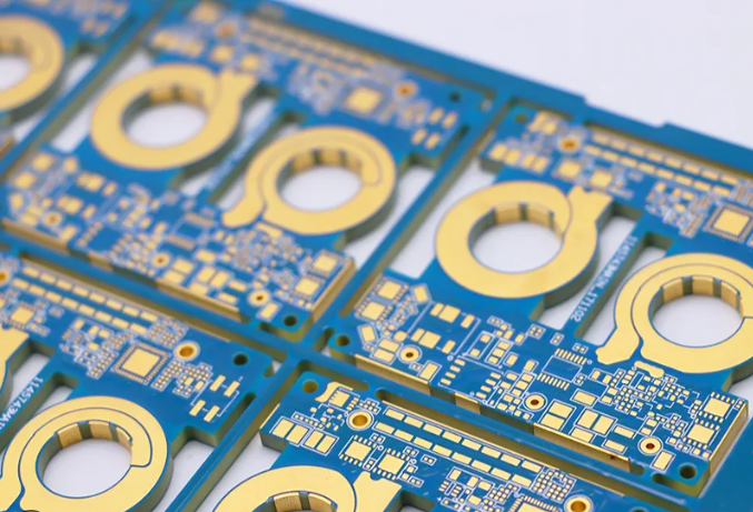
In contrast, multi-layer PCBs consist of multiple layers of conductive material separated by insulating layers, known as dielectric layers.
These additional layers allow for more complex and compact designs, as they provide ample space for routing numerous traces and interconnections. Multi-layer PCBs are indispensable in sophisticated electronic devices such as smartphones, computers, and medical equipment, where high performance and miniaturization are paramount.
One of the primary advantages of multi-layer PCBs is their ability to support higher circuit densities and more intricate designs.
The additional layers enable designers to implement advanced features such as power planes, ground planes, and signal layers, which enhance the overall performance and reliability of the circuit. Furthermore, the use of multiple layers reduces the need for long and convoluted traces, thereby minimizing signal loss and electromagnetic interference (EMI).
Despite their numerous benefits, multi-layer PCBs come with certain drawbacks.
The complexity of their design and manufacturing process results in higher production costs and longer lead times compared to single-layer PCBs. Additionally, the increased number of layers can make troubleshooting and repair more challenging, as identifying and accessing faulty components may require specialized equipment and expertise.
When deciding between single-layer and multi-layer PCB models, several factors must be considered.
The complexity of the circuit, the required performance, the available budget, and the intended application all play crucial roles in determining the most suitable PCB model. For simple, low-cost projects with minimal performance requirements, single-layer PCBs are often the preferred choice. Conversely, for advanced applications demanding high performance, compactness, and reliability, multi-layer PCBs are indispensable.
In conclusion, both single-layer and multi-layer PCB models have their unique advantages and limitations. Understanding these differences is essential for making informed decisions in electronic design and manufacturing. By carefully evaluating the specific needs of a project, designers can select the appropriate PCB model that best meets their requirements, ensuring optimal performance and cost-effectiveness.
Advanced Simulation Techniques For PCB Models
Advanced simulation techniques for PCB models have become indispensable in the modern electronics industry, where precision and reliability are paramount. As printed circuit boards (PCBs) grow increasingly complex, the need for sophisticated simulation tools to predict their behavior under various conditions has never been more critical. These advanced techniques not only enhance the design process but also significantly reduce the time and cost associated with prototyping and testing.
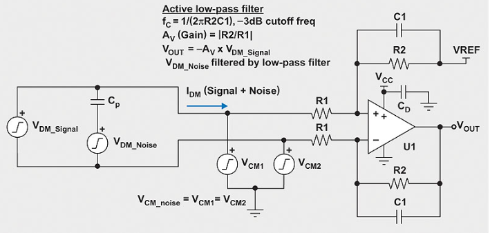
One of the primary simulation techniques employed in PCB modeling is electromagnetic (EM) simulation.
EM simulation allows engineers to analyze the electromagnetic fields and their interactions within the PCB. This is particularly important for high-frequency designs where signal integrity and electromagnetic compatibility (EMC) are crucial. By using EM simulation, designers can identify potential issues such as crosstalk, signal reflection, and radiation, which can adversely affect the performance of the PCB. Consequently, they can make informed decisions to mitigate these issues early in the design phase, thereby ensuring optimal performance.
In addition to EM simulation, thermal simulation plays a vital role in PCB modeling.
As electronic components become more powerful, they generate more heat, which can lead to thermal stress and potential failure if not properly managed. Thermal simulation enables designers to predict the temperature distribution across the PCB and identify hotspots that may require additional cooling measures. By incorporating thermal simulation into the design process, engineers can optimize the placement of components and heat sinks, ensuring that the PCB operates within safe temperature limits.
Another critical aspect of advanced simulation techniques is the use of signal integrity (SI) analysis.
SI analysis focuses on the quality of the electrical signals as they travel through the PCB traces. Poor signal integrity can result in data corruption, timing errors, and overall system instability. Through SI analysis, designers can evaluate the effects of various factors such as trace impedance, termination schemes, and via structures on signal quality. This allows them to fine-tune the PCB layout to minimize signal degradation and ensure reliable data transmission.
Moreover, power integrity (PI) analysis is essential for modern PCB designs, especially those with high-speed and high-density components.
PI analysis examines the distribution of power across the PCB and identifies areas where voltage drops or noise may occur. These issues can lead to malfunctioning components and reduced system performance. By conducting PI analysis, designers can optimize the power delivery network (PDN) to maintain stable voltage levels and minimize noise, thereby enhancing the overall reliability of the PCB.
Furthermore, advanced simulation techniques often involve the use of multi-physics simulations, which combine various physical phenomena such as electrical, thermal, and mechanical effects. Multi-physics simulations provide a comprehensive understanding of how different factors interact and influence the PCB’s performance. This holistic approach enables designers to address complex challenges that may not be apparent when considering each factor in isolation.
In conclusion, advanced simulation techniques for PCB models are essential tools that enable engineers to design high-performance, reliable, and cost-effective PCBs. By leveraging EM simulation, thermal simulation, SI analysis, PI analysis, and multi-physics simulations, designers can predict and mitigate potential issues early in the design process. This not only enhances the overall quality of the PCB but also accelerates the development cycle and reduces costs associated with prototyping and testing. As the electronics industry continues to evolve, the importance of these advanced simulation techniques will only grow, driving innovation and ensuring the success of future electronic devices.
Common Pitfalls In PCB Modeling And How To Avoid Them
Printed Circuit Board (PCB) modeling is a critical step in the design and manufacturing process of electronic devices. However, despite its importance, it is fraught with potential pitfalls that can lead to costly errors and delays. One common pitfall in PCB modeling is inadequate planning and design.
Often, designers rush into the modeling phase without thoroughly understanding the requirements and constraints of the project.
This can result in a PCB that does not meet the necessary specifications or fails to function as intended. To avoid this, it is essential to invest time in the initial planning stages, clearly defining the objectives, constraints, and performance criteria of the PCB.
Another frequent issue is the improper placement of components.
The layout of components on a PCB is crucial for its performance and reliability. Poor placement can lead to signal integrity problems, electromagnetic interference, and thermal issues. To mitigate this risk, designers should follow best practices for component placement, such as keeping high-speed signal paths short and ensuring adequate spacing between components to prevent overheating. Additionally, using simulation tools can help identify potential issues early in the design process.
Signal integrity is another area where PCB modeling can go awry.
High-speed circuits are particularly susceptible to signal integrity problems, such as crosstalk, reflection, and ground bounce. These issues can degrade the performance of the PCB and lead to malfunctioning devices. To address this, designers should pay close attention to the routing of high-speed signals, using techniques such as controlled impedance routing and differential pair routing. Furthermore, incorporating proper grounding and shielding practices can help minimize signal integrity issues.
Thermal management is a critical aspect of PCB design that is often overlooked.
Electronic components generate heat, and if this heat is not properly managed, it can lead to component failure and reduced lifespan of the PCB. Designers should consider the thermal properties of the materials used in the PCB and ensure that there is adequate heat dissipation. This can be achieved through the use of thermal vias, heat sinks, and proper airflow management. Additionally, thermal simulation tools can be used to predict and address potential thermal issues before the PCB is manufactured.
Manufacturability is another common pitfall in PCB modeling.
A design that looks good on paper may not be feasible to manufacture. Issues such as insufficient trace widths, inadequate spacing, and complex via structures can make the PCB difficult or impossible to produce. To avoid these problems, designers should adhere to the design for manufacturability (DFM) guidelines provided by the PCB manufacturer. This includes following the recommended design rules for trace widths, spacing, and via sizes, as well as considering the capabilities and limitations of the manufacturing process.
Lastly, documentation is a critical but often neglected aspect of PCB modeling.
Incomplete or inaccurate documentation can lead to misunderstandings and errors during the manufacturing process. To ensure a smooth transition from design to production, designers should provide comprehensive and accurate documentation, including schematics, layout files, bill of materials, and assembly drawings. Clear and detailed documentation helps communicate the design intent to the manufacturer and reduces the risk of errors.
In conclusion, while PCB modeling is a complex and challenging process, many common pitfalls can be avoided through careful planning, proper component placement, attention to signal integrity, effective thermal management, adherence to manufacturability guidelines, and thorough documentation. By addressing these areas, designers can create reliable and high-performance PCBs that meet the requirements of their projects.