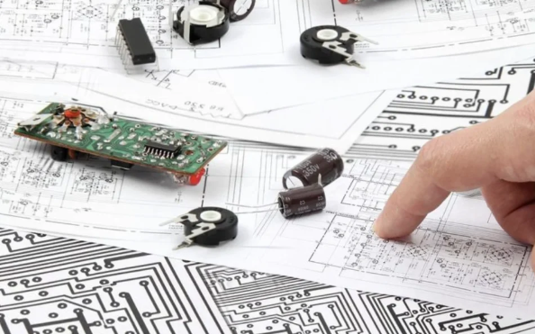
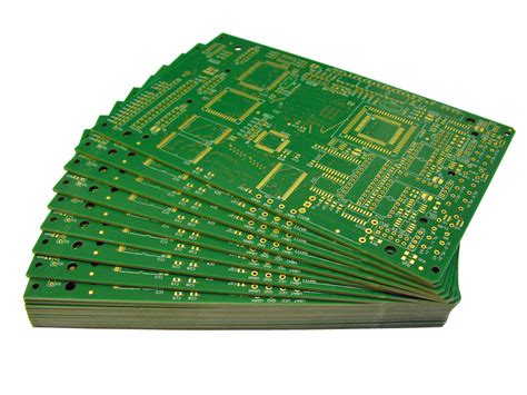
Mounting components on pcb
Surface Mount Technology: Techniques and Best Practices
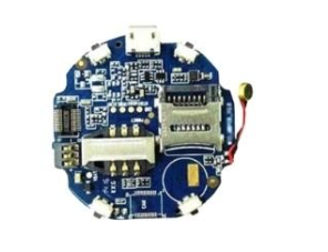
Surface Mount Technology (SMT) has revolutionized the electronics manufacturing industry by enabling the production of smaller, more efficient, and highly reliable electronic devices. This technique involves mounting components directly onto the surface of printed circuit boards (PCBs), eliminating the need for drilling holes as required in through-hole technology. As the demand for compact and complex electronic devices continues to grow, understanding the techniques and best practices for mounting components on PCBs using SMT becomes increasingly important.
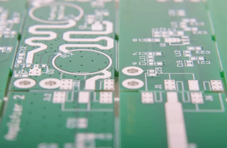
To begin with, the SMT process starts with the design and preparation of the PCB.
The board is typically coated with a solder mask to prevent solder bridges and to protect the copper traces. Following this, a layer of solder paste is applied to the pads on the PCB using a stencil. This paste, composed of tiny solder balls suspended in flux, serves as the adhesive that will hold the components in place and create electrical connections once melted. The precision of this step is crucial, as any misalignment can lead to defects in the final product.
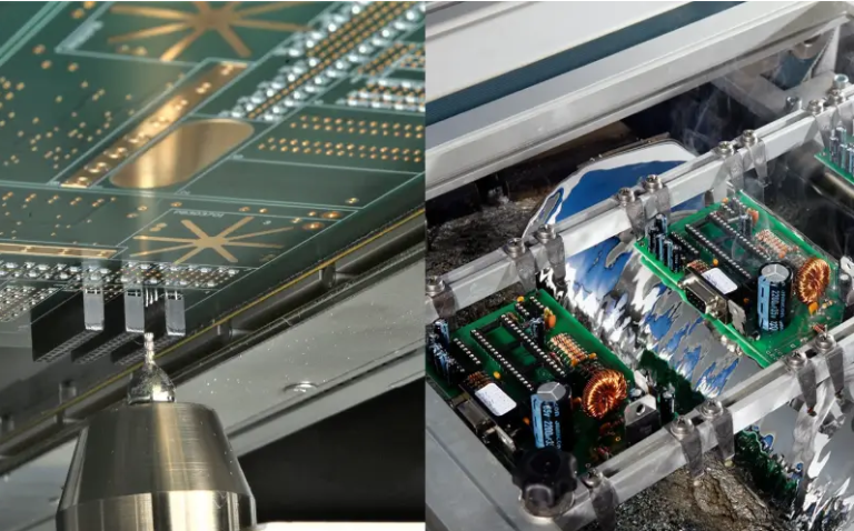
Once the solder paste is applied, the next step involves placing the components onto the PCB.
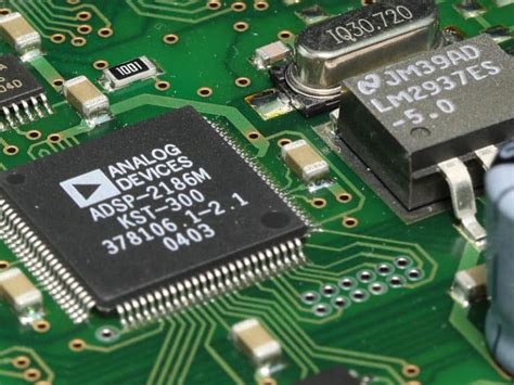
This is usually done using automated pick-and-place machines, which are programmed to position each component accurately based on the design specifications. These machines are capable of handling a wide range of component sizes and types, from tiny resistors and capacitors to larger integrated circuits. The speed and accuracy of these machines significantly enhance the efficiency of the SMT process, although manual placement may still be required for certain specialized components.
After the components are placed, the assembly is subjected to a reflow soldering process.
During this stage, the PCB is passed through a reflow oven where it is gradually heated to melt the solder paste. The molten solder forms a strong mechanical and electrical bond between the components and the PCB. It is essential to carefully control the temperature profile during reflow to prevent thermal damage to the components and ensure proper solder joint formation. This involves a series of heating and cooling phases, each with specific temperature and time requirements.
In addition to the technical aspects of SMT, adhering to best practices is vital for achieving high-quality results.
One such practice is ensuring the cleanliness of the PCB and components before assembly, as contaminants can lead to poor solder joints and reliability issues. Furthermore, selecting the appropriate solder paste and stencil design is crucial for achieving consistent results. The choice of materials and design parameters should be guided by the specific requirements of the application, such as thermal performance and mechanical strength.
Moreover, implementing a robust inspection and testing process is essential to identify and rectify any defects early in the production cycle.
Automated optical inspection (AOI) and X-ray inspection are commonly used to detect issues such as misalignment, insufficient solder, and voids in solder joints. These techniques provide valuable feedback that can be used to fine-tune the SMT process and improve overall yield.
In conclusion, Surface Mount Technology offers numerous advantages in the manufacturing of electronic devices, including reduced size, weight, and cost. By understanding and applying the techniques and best practices associated with SMT, manufacturers can produce high-quality PCBs that meet the demands of modern electronic applications. As technology continues to advance, staying informed about the latest developments in SMT will be crucial for maintaining a competitive edge in the electronics industry.
Through-Hole Mounting: Advantages and Applications
Through-hole mounting, a traditional method of attaching components to printed circuit boards (PCBs), remains a vital technique in the electronics industry despite the advent of surface-mount technology. This method involves inserting component leads through pre-drilled holes on the PCB and soldering them to pads on the opposite side. The enduring relevance of through-hole mounting can be attributed to its distinct advantages and specific applications where it outperforms other mounting techniques.
One of the primary advantages of through-hole mounting is its mechanical strength.
Components mounted using this method are securely fastened to the board, making them highly resistant to physical stress. This robustness is particularly beneficial in applications where the PCB may be subject to mechanical forces, such as in automotive, aerospace, and industrial equipment. The secure attachment ensures that components remain in place even under conditions of vibration or impact, thereby enhancing the reliability and longevity of the device.
Moreover, through-hole mounting facilitates easier manual assembly and prototyping.
The larger size of through-hole components and the visibility of their leads make them more accessible for technicians and engineers during the assembly process. This ease of handling is advantageous in situations where automated assembly is not feasible or when modifications and repairs are necessary. For prototyping, through-hole components allow for straightforward testing and iteration, enabling designers to make adjustments without the need for specialized equipment.
In addition to mechanical strength and ease of handling, through-hole mounting offers superior thermal performance.
The leads of through-hole components can dissipate heat more effectively than their surface-mount counterparts, which is crucial in high-power applications. This enhanced thermal management is essential in preventing overheating and ensuring the stable operation of electronic devices. Consequently, through-hole mounting is often preferred in power electronics, where efficient heat dissipation is a critical consideration.
Despite these advantages, it is important to acknowledge the limitations of through-hole mounting.
The requirement for drilled holes increases the complexity and cost of PCB manufacturing. Additionally, the larger size of through-hole components can limit the density of components on the board, making it less suitable for compact and lightweight devices. However, these drawbacks are often outweighed by the benefits in applications where reliability and durability are paramount.
Through-hole mounting finds its niche in various applications where its strengths are indispensable.
In military and aerospace sectors, the reliability and robustness of through-hole components are crucial for mission-critical systems. Similarly, in industrial settings, where equipment is exposed to harsh environments, the durability of through-hole mounted components ensures consistent performance. Furthermore, in educational and hobbyist projects, the simplicity and accessibility of through-hole components make them an ideal choice for learning and experimentation.
In conclusion, through-hole mounting continues to play a significant role in the electronics industry due to its unique advantages.
Its mechanical strength, ease of manual assembly, and superior thermal performance make it an invaluable technique in specific applications. While surface-mount technology has become the dominant method for many modern electronics, through-hole mounting remains indispensable in scenarios where reliability, durability, and ease of handling are critical. As technology advances, the complementary use of both mounting techniques will likely persist, each serving its purpose in the diverse landscape of electronic design and manufacturing.
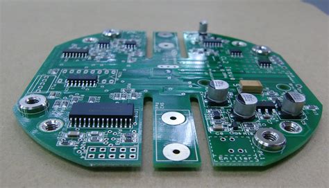
Mixed Technology PCB Assembly: Combining SMT and Through-Hole
In the realm of electronics manufacturing, the assembly of printed circuit boards (PCBs) is a critical process that demands precision and expertise. Among the various techniques employed, mixed technology PCB assembly stands out as a sophisticated method that combines Surface Mount Technology (SMT) and through-hole technology. This approach leverages the advantages of both techniques, allowing for the creation of complex and highly functional electronic devices. Understanding the nuances of mixed technology PCB assembly is essential for those involved in the design and production of modern electronic systems.
Surface Mount Technology, or SMT, is a method where components are mounted directly onto the surface of the PCB.
This technique is favored for its ability to accommodate a high density of components, making it ideal for compact and lightweight devices. SMT components are typically smaller and lighter than their through-hole counterparts, which allows for more efficient use of space on the PCB. Moreover, SMT facilitates automated assembly processes, which can significantly reduce production time and costs. However, despite these advantages, SMT is not without its limitations. For instance, it may not be suitable for components that require high mechanical strength or for applications that involve high power or high voltage.
On the other hand, through-hole technology involves inserting component leads through pre-drilled holes on the PCB and soldering them in place.
This method provides a robust mechanical bond, making it ideal for components that are subject to mechanical stress or require a strong connection. Through-hole technology is also preferred for components that need to dissipate heat effectively, as the leads can help conduct heat away from the component. Nevertheless, through-hole assembly is generally more labor-intensive and less suited for high-density applications compared to SMT.
In mixed technology PCB assembly, the strengths of both SMT and through-hole techniques are harnessed to create a versatile and efficient assembly process.
By integrating these two methods, manufacturers can optimize the performance and reliability of the final product. For instance, SMT can be used for the majority of components to achieve a compact design, while through-hole technology can be reserved for specific components that require additional mechanical support or thermal management.
The process of mixed technology assembly begins with careful planning and design.
Engineers must decide which components will be mounted using SMT and which will require through-hole assembly. This decision is influenced by factors such as the size and weight of the components, the required mechanical strength, and the thermal characteristics of the device. Once the design is finalized, the assembly process can commence, typically starting with the SMT components. These are placed and soldered using automated equipment, ensuring precision and efficiency. Following the SMT process, through-hole components are manually or semi-automatically inserted and soldered, completing the assembly.
In conclusion, mixed technology PCB assembly represents a strategic approach to electronic manufacturing, combining the best of SMT and through-hole techniques. This method not only enhances the functionality and reliability of electronic devices but also allows for greater design flexibility. As technology continues to evolve, the demand for sophisticated and efficient assembly methods like mixed technology PCB assembly is likely to grow, underscoring its importance in the field of electronics manufacturing.

Automated vs. Manual PCB Component Placement: Pros and Cons
In the realm of electronics manufacturing, the process of mounting components on printed circuit boards (PCBs) is a critical step that significantly influences the performance and reliability of the final product. This process can be executed through either automated or manual methods, each offering distinct advantages and disadvantages. Understanding these differences is essential for manufacturers aiming to optimize their production processes.
Automated PCB component placement, often referred to as pick-and-place technology, utilizes sophisticated machinery to position components onto the board with high precision and speed.
One of the primary advantages of automation is its efficiency. Automated systems can place thousands of components per hour, far surpassing the capabilities of manual labor. This speed is particularly beneficial for large-scale production, where time is a critical factor. Moreover, automated placement ensures a high degree of accuracy and consistency, reducing the likelihood of human error. This precision is crucial for complex PCBs with densely packed components, where even a slight misalignment can lead to functional issues.
In addition to speed and accuracy, automated systems offer the advantage of scalability.
As production demands increase, automated systems can be easily adjusted to accommodate higher volumes without a proportional increase in labor costs. Furthermore, these systems can operate continuously, limited only by maintenance schedules, thus maximizing throughput. However, despite these benefits, automated placement is not without its drawbacks. The initial investment in machinery and setup can be substantial, making it less feasible for small-scale operations or startups with limited capital. Additionally, automated systems may struggle with highly customized or intricate designs that require a level of dexterity and adaptability that machines cannot yet replicate.
On the other hand, manual PCB component placement involves skilled technicians placing components by hand.
This method offers a level of flexibility that automated systems cannot match. For prototypes or small production runs, manual placement allows for quick adjustments and modifications without the need for extensive reprogramming or setup changes. This adaptability is particularly advantageous in research and development settings, where designs frequently evolve. Moreover, manual placement can be more cost-effective for low-volume production, as it eliminates the need for expensive machinery and reduces overhead costs associated with maintenance and operation.
However, manual placement is not without its limitations.
The process is inherently slower than automated methods, which can lead to longer production times and increased labor costs. Additionally, the reliance on human operators introduces the potential for errors, which can compromise the quality and reliability of the final product. As the complexity of PCBs increases, the risk of misplacement or damage during manual handling also rises, necessitating rigorous quality control measures.
In conclusion, the choice between automated and manual PCB component placement hinges on several factors, including production volume, budget, and design complexity. Automated systems offer unparalleled speed and precision, making them ideal for large-scale manufacturing. In contrast, manual placement provides flexibility and cost-effectiveness for smaller operations or projects requiring frequent design changes. Ultimately, manufacturers must carefully evaluate their specific needs and resources to determine the most suitable approach, balancing the benefits and limitations of each method to achieve optimal results.