Multilayer pcb basics
Introduction To Multilayer PCB Design
Multilayer printed circuit boards (PCBs) have become a cornerstone in the design and manufacturing of modern electronic devices. As technology continues to advance, the demand for more compact, efficient, and powerful electronic components has driven the evolution from single-layer to multilayer PCBs. Understanding the basics of multilayer PCB design is essential for engineers and designers who aim to create sophisticated electronic systems.
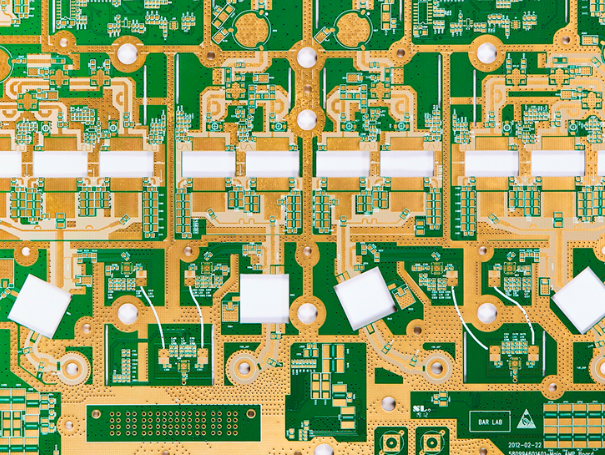
At its core, a multilayer PCB consists of multiple layers of conductive material, typically copper, separated by insulating layers known as dielectric materials.
These layers are laminated together under high pressure and temperature to form a single, cohesive unit. The primary advantage of this structure is the ability to incorporate a greater number of circuits within a smaller footprint, which is crucial for the miniaturization of electronic devices.
One of the fundamental aspects of multilayer PCB design is the stack-up configuration.
The stack-up refers to the arrangement and sequence of conductive and insulating layers within the PCB. A well-designed stack-up can significantly impact the electrical performance, signal integrity, and electromagnetic compatibility of the final product. Typically, a multilayer PCB will have at least four layers, including two outer layers and two or more inner layers. The outer layers are usually reserved for component placement and routing, while the inner layers are used for power distribution and signal routing.
Transitioning from single-layer to multilayer PCBs introduces several design considerations.
For instance, designers must carefully plan the routing of signals to minimize interference and crosstalk between adjacent layers. This often involves the use of ground planes, which are continuous layers of conductive material that serve as a common return path for electrical currents. Ground planes help to reduce electromagnetic interference and improve signal integrity by providing a low-impedance path for return currents.
Another critical aspect of multilayer PCB design is the management of thermal performance.
As electronic components become more densely packed, the potential for heat buildup increases, which can adversely affect the reliability and lifespan of the device. To address this, designers must consider the thermal conductivity of the materials used and incorporate thermal vias—small holes filled with conductive material that facilitate heat dissipation between layers.
Moreover, the choice of materials plays a pivotal role in the performance of multilayer PCBs.
The dielectric material must possess specific electrical properties, such as dielectric constant and loss tangent, to ensure optimal signal transmission. Additionally, the copper thickness on each layer must be carefully selected to handle the required current load without causing excessive heat generation.
In conclusion, the design of multilayer PCBs is a complex process that requires a deep understanding of electrical, thermal, and material properties. As electronic devices continue to evolve, the demand for more sophisticated multilayer PCBs will only increase. By mastering the basics of multilayer PCB design, engineers and designers can create innovative solutions that meet the ever-growing needs of the electronics industry. Through careful consideration of stack-up configurations, signal routing, thermal management, and material selection, multilayer PCBs can be optimized to deliver superior performance and reliability in a wide range of applications.

Advantages Of Multilayer PCBs Over Single-Layer Boards
Multilayer printed circuit boards (PCBs) have become a cornerstone in modern electronics, offering numerous advantages over their single-layer counterparts. As technology continues to advance, the demand for more compact, efficient, and powerful electronic devices has driven the evolution of PCB design. Multilayer PCBs, which consist of multiple layers of conductive material separated by insulating layers, provide a solution to many of the limitations inherent in single-layer boards.
One of the primary advantages of multilayer PCBs is their ability to support higher component density.
In single-layer boards, the available surface area is limited, which restricts the number of components that can be mounted. Multilayer PCBs, however, allow for the stacking of multiple layers, effectively increasing the available surface area without expanding the board’s footprint. This capability is particularly beneficial in applications where space is at a premium, such as in smartphones, laptops, and other portable devices.
Moreover, multilayer PCBs offer enhanced electrical performance.
The additional layers provide more routing options for signal paths, which can significantly reduce the length of connections between components. This reduction in path length minimizes signal loss and electromagnetic interference, leading to improved signal integrity and overall performance. Furthermore, the ability to incorporate ground and power planes within the layers helps in stabilizing voltage levels and reducing noise, which is crucial for high-speed and high-frequency applications.
In addition to improved electrical performance, multilayer PCBs contribute to greater design flexibility.
Designers can implement more complex circuit designs by utilizing the multiple layers to separate different functions or signal types. This separation allows for better organization and management of the circuit, facilitating easier troubleshooting and modifications. The flexibility in design also enables the integration of advanced features and functionalities that would be challenging to achieve with single-layer boards.
Another significant advantage of multilayer PCBs is their durability and reliability.
The construction of these boards involves pressing and bonding multiple layers together, resulting in a robust structure that can withstand mechanical stress and environmental factors better than single-layer boards. This durability is essential in applications where the PCB may be subjected to harsh conditions, such as in automotive or industrial environments.
Furthermore, multilayer PCBs can lead to cost savings in the long run.
Although the initial manufacturing cost of multilayer boards may be higher due to the complexity of their design and production processes, the benefits they offer can outweigh these costs. The increased component density and improved performance can lead to smaller, more efficient devices, which can reduce material and production costs. Additionally, the enhanced reliability and durability of multilayer PCBs can result in lower maintenance and replacement costs over the device’s lifespan.
In conclusion, multilayer PCBs present a multitude of advantages over single-layer boards, making them an indispensable component in modern electronic design.
Their ability to support higher component density, improve electrical performance, offer design flexibility, and provide durability and reliability makes them a preferred choice for a wide range of applications. As technology continues to evolve, the role of multilayer PCBs in enabling more advanced and efficient electronic devices is likely to become even more significant.
Key Considerations In Multilayer PCB Manufacturing
In the realm of electronics, multilayer printed circuit boards (PCBs) have become indispensable due to their ability to support complex and high-density designs. As the demand for more compact and efficient electronic devices grows, understanding the key considerations in multilayer PCB manufacturing becomes crucial for engineers and manufacturers alike. The process of creating these intricate boards involves several critical steps, each requiring meticulous attention to detail to ensure optimal performance and reliability.
To begin with, the design phase is paramount in multilayer PCB manufacturing.
Engineers must carefully plan the layout, considering factors such as signal integrity, thermal management, and electromagnetic interference. The number of layers in a PCB is determined by the complexity of the circuit and the need for additional routing space. Typically, multilayer PCBs consist of three or more layers of conductive material, separated by insulating layers. This configuration allows for more intricate designs and greater functionality within a smaller footprint.
Once the design is finalized, material selection becomes a key consideration.
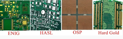
The choice of materials impacts the board’s performance, durability, and cost. Common materials used in multilayer PCBs include FR-4, a glass-reinforced epoxy laminate, and polyimide, known for its flexibility and high thermal resistance. The dielectric constant and loss tangent of these materials must be carefully evaluated to ensure they meet the specific requirements of the application. Additionally, the copper thickness for each layer must be determined, as it affects the board’s current-carrying capacity and overall thermal performance.
The manufacturing process itself involves several intricate steps, starting with the creation of the inner layers.
These layers are etched with the desired circuit pattern using a photolithographic process. Once the inner layers are prepared, they are laminated together under heat and pressure, with insulating layers in between. This lamination process is critical, as it ensures the structural integrity and electrical isolation of the board. After lamination, the outer layers are added, and the entire stack is drilled to create vias, which are essential for interconnecting the different layers.
Quality control is another vital aspect of multilayer PCB manufacturing.
Each board must undergo rigorous testing to ensure it meets the required specifications. Electrical testing, such as continuity and isolation tests, is performed to verify the integrity of the circuits. Additionally, inspection techniques like automated optical inspection (AOI) and X-ray inspection are employed to detect any defects or misalignments that could compromise the board’s functionality.
Furthermore, environmental considerations play a significant role in the manufacturing process.
As electronic devices become more prevalent, the industry faces increasing pressure to adopt sustainable practices. This includes minimizing waste, reducing energy consumption, and using environmentally friendly materials. Manufacturers are also exploring lead-free soldering techniques and other green initiatives to align with global environmental standards.
In conclusion, multilayer PCB manufacturing is a complex process that requires careful consideration of various factors, from design and material selection to quality control and environmental impact. As technology continues to advance, the demand for more sophisticated and compact electronic devices will drive further innovation in this field. By understanding the intricacies of multilayer PCB manufacturing, engineers and manufacturers can ensure the production of high-quality boards that meet the ever-evolving needs of the electronics industry.
Common Applications Of Multilayer PCBs In Modern Electronics
Multilayer printed circuit boards (PCBs) have become a cornerstone in the design and functionality of modern electronic devices. As technology continues to advance, the demand for more compact, efficient, and powerful electronic components has led to the widespread adoption of multilayer PCBs. These sophisticated boards, which consist of multiple layers of conductive material separated by insulating layers, offer numerous advantages over their single-layer counterparts. Consequently, they have found applications in a wide array of electronic devices, each benefiting from the unique properties that multilayer PCBs provide.
One of the most prevalent applications of multilayer PCBs is in the realm of consumer electronics.
Devices such as smartphones, tablets, and laptops rely heavily on these complex boards to meet the ever-increasing demand for enhanced performance and miniaturization. The compact nature of multilayer PCBs allows for the integration of more components within a smaller footprint, which is essential for the sleek and portable designs that consumers expect. Furthermore, the improved electrical performance and reduced electromagnetic interference offered by multilayer PCBs contribute to the overall efficiency and reliability of these devices.
In addition to consumer electronics, multilayer PCBs play a crucial role in the telecommunications industry.
As the backbone of modern communication systems, these boards are integral to the operation of routers, switches, and other networking equipment. The ability to handle high-speed signals and support complex routing requirements makes multilayer PCBs ideal for these applications. Moreover, the increased layer count allows for greater signal integrity and reduced crosstalk, which are vital for maintaining the quality and speed of data transmission in telecommunications networks.
The automotive industry also benefits significantly from the use of multilayer PCBs.
With the rise of electric vehicles and the growing complexity of automotive electronics, these boards are essential for managing the intricate systems found in modern cars. From engine control units to advanced driver-assistance systems, multilayer PCBs provide the necessary support for the sophisticated electronics that enhance vehicle performance, safety, and connectivity. The durability and reliability of multilayer PCBs are particularly important in automotive applications, where components must withstand harsh environmental conditions and rigorous operational demands.
Moreover, multilayer PCBs are indispensable in the medical field, where precision and reliability are paramount.
Medical devices such as imaging systems, patient monitoring equipment, and implantable devices rely on multilayer PCBs to function effectively. The compact design and high-density interconnections offered by these boards enable the development of smaller, more efficient medical devices that can deliver accurate diagnostics and treatment. Additionally, the ability to incorporate multiple functionalities into a single board reduces the complexity and potential for failure, which is critical in life-saving medical applications.
Finally, the aerospace and defense sectors utilize multilayer PCBs for their advanced electronic systems.
The stringent requirements for performance, reliability, and weight reduction in these industries make multilayer PCBs an ideal choice. From avionics systems to radar and communication equipment, these boards provide the necessary support for the sophisticated technologies that drive modern aerospace and defense applications. The ability to withstand extreme temperatures and environmental conditions further underscores the suitability of multilayer PCBs for these demanding applications.
In conclusion, the versatility and advanced capabilities of multilayer PCBs have made them an integral component in a wide range of modern electronic applications. As technology continues to evolve, the role of multilayer PCBs in enabling innovation and enhancing performance across various industries is likely to expand, further solidifying their importance in the world of electronics.