Multilayer RF PCB Design: Challenges, Techniques, and Best Practices
In the rapidly evolving field of wireless communication, radio frequency (RF) printed circuit boards (PCBs) play a critical role in enabling high-performance devices such as 5G networks, satellite systems, radar, and IoT devices. Multilayer RF PCBs, in particular, are essential for complex designs that require high signal integrity, minimal interference, and efficient thermal management. However, designing multilayer RF PCBs presents unique challenges due to the high-frequency nature of the signals and the complexity of managing multiple layers. This article explores the key aspects of multilayer RF PCB design, including challenges, techniques, and best practices to achieve optimal performance.
What Are Multilayer RF PCBs?
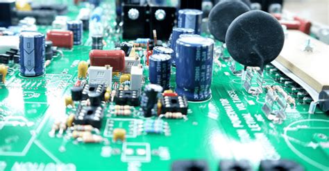
Multilayer RF PCBs are circuit boards with three or more layers of conductive material separated by dielectric layers. These PCBs are specifically designed to handle high-frequency signals, typically in the range of hundreds of megahertz (MHz) to several gigahertz (GHz). The multiple layers allow for better signal routing, reduced electromagnetic interference (EMI), and improved thermal performance, making them ideal for advanced RF applications.
Key Challenges in Multilayer RF PCB Design
Designing multilayer RF PCBs involves addressing several challenges that are not typically encountered in low-frequency or digital PCB designs. These challenges include:
1.Signal Integrity:
- High-frequency signals are susceptible to losses, reflections, and distortions, which can degrade performance.
- Maintaining consistent impedance and minimizing signal loss are critical for ensuring signal integrity.
- Electromagnetic Interference (EMI):
- RF circuits are prone to EMI, both as sources and victims of interference.
- Proper shielding and grounding are essential to minimize EMI.
- Thermal Management:
- High-frequency circuits often generate significant heat, which must be effectively dissipated to prevent component failure.
- Multilayer designs require careful planning to manage heat distribution.
- Material Selection:
- The choice of substrate material significantly impacts the performance of RF PCBs.
- Materials with low dielectric loss and stable electrical properties are preferred.
- Complex Routing:
- Routing high-frequency signals in a multilayer PCB requires careful planning to avoid crosstalk and ensure proper impedance matching.
- Manufacturing Tolerances:
- High-frequency designs demand tight manufacturing tolerances, which can increase production costs and complexity.
Key Techniques for Multilayer RF PCB Design
To overcome the challenges of multilayer RF PCB design, engineers employ a variety of techniques and best practices. These techniques ensure optimal performance, reliability, and manufacturability.
1. Impedance Control
- Impedance Matching: Ensure that the characteristic impedance of transmission lines (e.g., microstrips or striplines) matches the system impedance (typically 50 ohms for RF applications).
- Controlled Dielectric Thickness: Use precise dielectric thicknesses to achieve consistent impedance across the PCB.
- Simulation Tools: Utilize electromagnetic simulation software to model and optimize impedance.
2. Layer Stackup Design
- Signal Layers: Place high-frequency signal layers adjacent to ground planes to minimize EMI and provide a return path for currents.
- Ground Planes: Use solid ground planes to reduce noise and provide shielding.
- Power Planes: Distribute power evenly across the PCB and decouple power supplies to minimize noise.
3. Material Selection
- Low-Dk Materials: Choose materials with a low dielectric constant (Dk) to minimize signal delay and loss.
- Low-Df Materials: Select materials with a low dissipation factor (Df) to reduce signal attenuation.
- Thermal Properties: Consider materials with high thermal conductivity for effective heat dissipation.
4. Routing Best Practices
- Short Traces: Keep high-frequency traces as short as possible to minimize losses and reflections.
- Avoid Sharp Corners: Use curved or 45-degree angles for traces to reduce impedance discontinuities.
- Differential Pairs: Route differential pairs closely together to maintain signal integrity and reduce EMI.
5. Shielding and Grounding
- Via Stitching: Use via stitching to connect ground planes and create a Faraday cage around sensitive components.
- Shielding Cans: Add shielding cans to isolate high-frequency components and reduce EMI.
- Split Ground Planes: Avoid splitting ground planes, as this can create impedance mismatches and increase noise.
6. Thermal Management
- Thermal Vias: Use thermal vias to transfer heat from high-power components to other layers or heat sinks.
- Copper Pours: Add copper pours to dissipate heat and improve thermal performance.
- Heat Sinks: Integrate heat sinks or thermal pads for components that generate significant heat.
7. Testing and Validation
- Prototype Testing: Build and test prototypes to validate the design and identify potential issues.
- Signal Integrity Analysis: Perform signal integrity analysis to ensure proper impedance matching and minimize losses.
- EMI Testing: Conduct EMI testing to verify compliance with regulatory standards.
Best Practices for Multilayer RF PCB Design
To achieve optimal performance in multilayer RF PCB designs, follow these best practices:
- Collaborate with Manufacturers:
- Work closely with PCB manufacturers to ensure that the design meets their capabilities and tolerances.
- Discuss material options, layer stackup, and manufacturing constraints early in the design process.
- Use Advanced Design Tools:
- Leverage advanced PCB design software with RF-specific features, such as impedance calculators, electromagnetic simulators, and signal integrity analysis tools.
- Minimize Crosstalk:
- Separate high-frequency signals from low-frequency signals and digital signals to reduce crosstalk.
- Use guard traces or ground planes between sensitive signals.
- Optimize Component Placement:
- Place high-frequency components close to each other to minimize trace lengths.
- Group components by function to simplify routing and reduce interference.
- Plan for Testing:
- Include test points and access points in the design to facilitate debugging and validation.
- Design for manufacturability (DFM) to ensure that the PCB can be easily tested and assembled.
- Follow Industry Standards:
- Adhere to industry standards and guidelines, such as IPC-2221 and IPC-2141, for RF PCB design.
- Ensure compliance with regulatory requirements for EMI and safety.
Applications of Multilayer RF PCBs
Multilayer RF PCBs are used in a wide range of high-frequency applications, including:
- 5G Networks:
- Multilayer RF PCBs are essential for 5G base stations, antennas, and transceivers, which require high signal integrity and low loss.
- Satellite Communication:
- Satellite systems rely on multilayer RF PCBs for signal processing, amplification, and transmission.
- Radar Systems:
- Radar systems use multilayer RF PCBs for high-frequency signal generation, processing, and detection.
- IoT Devices:
- IoT devices, such as smart sensors and wireless modules, require compact and efficient multilayer RF PCBs.
- Medical Equipment:
- Medical devices, such as MRI machines and wireless monitoring systems, use multilayer RF PCBs for reliable and high-performance operation.
Future Trends in Multilayer RF PCB Design
As technology continues to advance, several trends are shaping the future of multilayer RF PCB design:
- Higher Frequencies:
- The demand for higher frequencies, such as millimeter-wave (mmWave) bands, is driving the development of advanced materials and design techniques.
- Integration with Advanced Technologies:
- Multilayer RF PCBs are being integrated with technologies such as 3D printing, flexible circuits, and embedded components.
- Miniaturization:
- The trend toward smaller and more compact devices is pushing the limits of multilayer RF PCB design, requiring innovative solutions for routing and thermal management.
- Sustainability:
- There is a growing focus on using environmentally friendly materials and processes in PCB manufacturing.
Conclusion
Multilayer RF PCB design is a complex and challenging field that requires a deep understanding of high-frequency signals, material properties, and advanced design techniques. By addressing key challenges such as signal integrity, EMI, and thermal management, and following best practices for layer stackup, routing, and testing, engineers can create high-performance RF PCBs that meet the demands of modern wireless communication systems.
As the demand for faster, more reliable, and more compact devices continues to grow, the importance of multilayer RF PCB design will only increase. By staying informed about the latest trends and technologies, designers can push the boundaries of what is possible and enable the next generation of wireless innovation.


