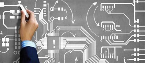
New Technologies in PCB Cloning and Design
Introduction
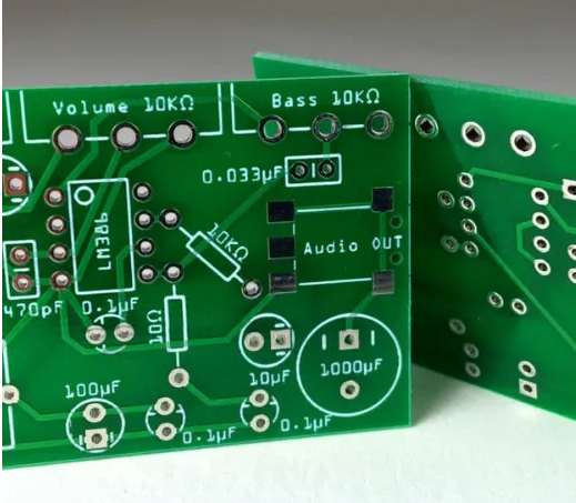
Printed Circuit Board (PCB) cloning, also known as PCB copying or reverse engineering, is the process of analyzing an existing PCB to recreate its design, schematics, and layout. This practice is widely used in industries such as electronics manufacturing, repair, and prototyping. With advancements in technology, PCB cloning has evolved significantly, incorporating new techniques that improve accuracy, efficiency, and cost-effectiveness.
This article explores the latest innovations in PCB cloning and design, including automated scanning, AI-assisted reverse engineering, 3D imaging, and advanced software tools. These technologies are transforming the way engineers and manufacturers approach PCB replication and optimization.
1. Automated PCB Scanning and Imaging
Traditional PCB cloning involved manual tracing of circuits, which was time-consuming and prone to errors. Modern techniques leverage high-resolution scanning and imaging to digitize PCBs efficiently.
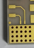
High-Resolution Optical Scanning
- Laser Scanning & Photogrammetry: Advanced scanners capture detailed images of PCB layers, including traces, vias, and components.
- X-Ray Imaging: For multi-layer PCBs, X-ray tomography provides internal layer visualization without physical disassembly.
- 3D Scanning: Structured-light 3D scanners reconstruct PCB topography, helping in component placement analysis.
Automated Trace Extraction
- Software like Altium Designer and KiCad can convert scanned images into editable PCB layouts.
- Machine vision algorithms detect traces, pads, and silkscreen markings automatically.
2. AI and Machine Learning in PCB Reverse Engineering
Artificial Intelligence (AI) is revolutionizing PCB cloning by automating complex tasks that previously required human expertise.
Automated Schematic Generation
- AI-powered tools analyze PCB images and generate netlists and schematics automatically.
- Deep learning models recognize component footprints and connections, reducing manual effort.
Component Identification
- AI algorithms classify components (resistors, ICs, capacitors) and suggest datasheets.
- OCR (Optical Character Recognition) extracts part numbers and labels from PCBs.
Signal Path Prediction
- AI predicts signal flow and power distribution, aiding in debugging cloned designs.
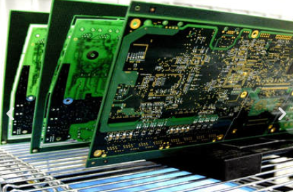
3. Advanced PCB Design Software for Cloning
Modern PCB design tools integrate cloning functionalities, making reverse engineering more efficient.
Key Software Solutions
- Altium Designer – Supports PCB import from images and auto-routing for cloned designs.
- Cadence OrCAD – Features schematic reconstruction from physical PCBs.
- KiCad – Open-source tool with image-to-PCB conversion plugins.
- PADS – Allows layer-by-layer analysis for multi-layer PCBs.
Automated DFM (Design for Manufacturing) Checks
- Cloned designs are verified for manufacturability, preventing errors before production.
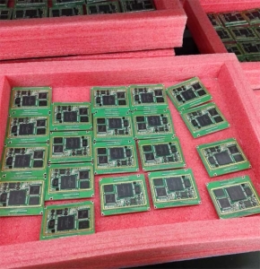
4. 3D Printing and Rapid PCB Prototyping
3D printing technology is being integrated into PCB cloning for faster prototyping.
Hybrid PCB Fabrication
- Conductive ink printing allows direct PCB trace deposition on substrates.
- Aerosol Jet Printing enables fine-pitch component placement.
3D-Printed Circuit Boards
- Multi-material 3D printers create PCBs with embedded components.
- Flexible and stretchable PCBs can be prototyped using additive manufacturing.
5. Blockchain for Secure PCB Cloning
With concerns about intellectual property (IP) theft, blockchain technology is being used to secure PCB designs.
Digital Fingerprinting
- Each PCB design is hashed and stored on a blockchain to verify authenticity.
- Smart contracts control access to cloned designs, ensuring authorized use only.
Anti-Cloning Measures
- Manufacturers embed cryptographic markers in PCBs to prevent unauthorized replication.
6. Cloud-Based PCB Collaboration Platforms
Cloud computing enables collaborative PCB cloning and design across global teams.
Real-Time Collaboration
- Engineers share and edit PCB designs simultaneously via platforms like Altium 365.
- Version control ensures traceability of design modifications.
AI-Powered Cloud Analysis
- Cloud-based AI tools analyze PCB scans and suggest optimizations.
Conclusion
PCB cloning has transitioned from a manual, error-prone process to a highly automated and intelligent workflow. Technologies such as AI-assisted reverse engineering, 3D imaging, advanced PCB software, and blockchain security are reshaping the industry. These innovations not only accelerate PCB replication but also enhance accuracy, security, and manufacturability.
As electronics continue to evolve, PCB cloning techniques will further integrate with IoT, AI, and advanced fabrication methods, enabling faster prototyping and more efficient electronics production. Companies adopting these new technologies will gain a competitive edge in rapid product development and repair services