Nfc flex pcb antenna
Design Considerations for NFC Flex PCB Antennas
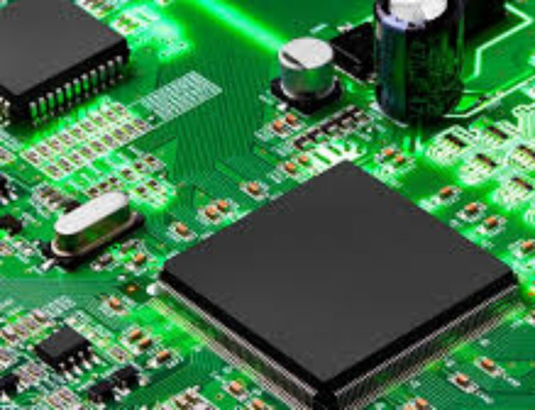
When designing NFC flex PCB antennas, several critical considerations must be taken into account to ensure optimal performance and functionality. The integration of NFC technology into flexible printed circuit boards (PCBs) offers numerous advantages, including enhanced durability, reduced weight, and the ability to conform to various shapes and surfaces. However, these benefits come with unique challenges that require careful attention during the design process.
To begin with, the choice of materials is paramount in the design of NFC flex PCB antennas.
The substrate material must be flexible yet robust enough to withstand repeated bending and flexing without compromising the antenna’s performance. Polyimide is a popular choice due to its excellent thermal stability and mechanical properties. Additionally, the conductive materials used for the antenna traces, typically copper, must be selected to ensure minimal resistance and optimal signal transmission.
Moreover, the antenna’s geometry plays a crucial role in its performance.
The size and shape of the antenna must be carefully designed to match the specific frequency requirements of the NFC application, typically around 13.56 MHz. The antenna’s inductance and capacitance must be precisely calculated to achieve the desired resonant frequency, which is essential for efficient energy transfer between the NFC reader and the tag. This involves a delicate balance between the antenna’s physical dimensions and its electrical characteristics.
Transitioning to the layout considerations, the placement of the antenna on the flex PCB is another critical factor.
The antenna should be positioned to minimize interference from other components and to maximize its exposure to the NFC reader’s electromagnetic field. This often involves strategic placement away from metal objects and other potential sources of electromagnetic interference. Additionally, the antenna’s orientation relative to the NFC reader must be considered to ensure consistent performance across different use cases.
Furthermore, the integration of the NFC antenna with other components on the flex PCB requires careful planning.
The antenna must be electrically isolated from other circuits to prevent signal degradation and ensure reliable communication. This can be achieved through the use of ground planes and shielding techniques, which help to minimize crosstalk and electromagnetic interference. Additionally, the antenna’s connection to the NFC controller chip must be designed to minimize signal loss and ensure efficient power transfer.
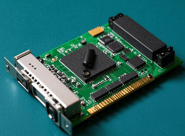
In addition to these technical considerations, manufacturability is an important aspect of NFC flex PCB antenna design.
The design must be optimized for mass production, taking into account factors such as material availability, manufacturing tolerances, and assembly processes. This often involves collaboration with manufacturing partners to ensure that the design can be produced cost-effectively and at scale.
Finally, testing and validation are essential steps in the design process.
Prototyping and rigorous testing under various conditions help to identify potential issues and ensure that the antenna meets the required performance specifications. This includes testing for durability, signal integrity, and compatibility with different NFC readers and devices.
In conclusion, the design of NFC flex PCB antennas involves a complex interplay of material selection, geometric design, layout considerations, and manufacturability. By carefully addressing these factors, designers can create antennas that deliver reliable performance and meet the demands of modern NFC applications. As NFC technology continues to evolve, ongoing research and development will further enhance the capabilities and applications of flex PCB antennas, paving the way for innovative solutions in a wide range of industries.
Innovative Applications of NFC Flex PCB Antennas in IoT
The rapid advancement of technology in recent years has paved the way for the Internet of Things (IoT) to become an integral part of our daily lives. Among the various components that facilitate the seamless connectivity of IoT devices, Near Field Communication (NFC) technology stands out due to its ability to enable secure and efficient data exchange over short distances. A critical element in the functionality of NFC systems is the antenna, and the development of NFC flexible printed circuit board (PCB) antennas has opened up a myriad of innovative applications within the IoT landscape.
NFC flex PCB antennas are designed to be lightweight, thin, and highly adaptable, making them ideal for integration into a wide range of devices.
Their flexibility allows them to conform to various shapes and surfaces, which is particularly advantageous in the design of wearable technology. For instance, smartwatches and fitness trackers can incorporate NFC flex PCB antennas to facilitate contactless payments, access control, and data synchronization with other smart devices. This adaptability not only enhances the user experience but also expands the potential for creative design in wearable tech.
Moreover, the use of NFC flex PCB antennas extends beyond wearables into the realm of smart home devices.
As homes become increasingly connected, the demand for efficient communication between devices grows. NFC technology, with its low power consumption and secure data transfer capabilities, is well-suited for this environment. Flex PCB antennas can be embedded into smart locks, lighting systems, and home appliances, enabling users to control and monitor their home environment with ease. The integration of NFC technology in these devices allows for seamless interaction and automation, contributing to the overall convenience and efficiency of smart homes.
In addition to consumer electronics, NFC flex PCB antennas are finding applications in the healthcare sector.
Medical devices equipped with NFC technology can offer improved patient monitoring and data management. For example, NFC-enabled sensors can be used to track vital signs and transmit data to healthcare providers in real-time. The flexibility of the PCB antennas ensures that these sensors can be comfortably worn by patients, enhancing compliance and the accuracy of the data collected. Furthermore, NFC technology can facilitate secure access to medical records and streamline the process of medication administration, thereby improving patient care and safety.
The retail industry is also benefiting from the innovative applications of NFC flex PCB antennas.
Retailers are increasingly adopting NFC technology to enhance the shopping experience through contactless payment systems and smart shelves. Flex PCB antennas can be integrated into product packaging, allowing consumers to access detailed product information and promotions with a simple tap of their smartphone. This not only enriches the shopping experience but also provides retailers with valuable insights into consumer behavior and preferences.
As the IoT ecosystem continues to expand, the role of NFC flex PCB antennas in enabling efficient and secure communication between devices becomes increasingly significant. Their versatility and adaptability make them a key component in the development of innovative solutions across various industries. By facilitating seamless connectivity and interaction, NFC flex PCB antennas are helping to drive the evolution of IoT, ultimately transforming the way we live and interact with technology. As research and development in this field progress, we can anticipate even more groundbreaking applications that will further integrate NFC technology into the fabric of our connected world.

Challenges and Solutions in Manufacturing NFC Flex PCB Antennas
The manufacturing of NFC (Near Field Communication) flex PCB (Printed Circuit Board) antennas presents a unique set of challenges and solutions that are critical to the advancement of modern communication technologies. As NFC technology becomes increasingly integral to a wide range of applications, from contactless payments to smart home devices, the demand for efficient and reliable flex PCB antennas continues to grow. However, the production of these components is not without its difficulties, which stem from the intricate balance of material properties, design constraints, and manufacturing processes.
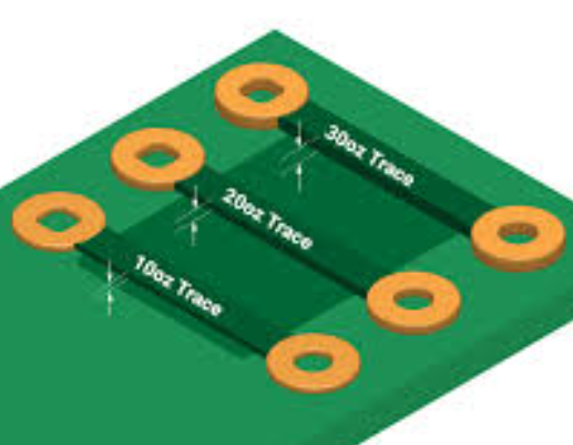
One of the primary challenges in manufacturing NFC flex PCB antennas is the selection of appropriate materials.
The materials used must exhibit excellent electrical conductivity while maintaining flexibility and durability. Copper is commonly used due to its superior conductive properties, but it must be carefully laminated onto a flexible substrate, such as polyimide, to ensure the antenna can withstand bending and twisting without compromising performance. This requirement necessitates precise control over the lamination process to prevent delamination or cracking, which can lead to signal loss or complete failure of the antenna.
In addition to material selection, the design of NFC flex PCB antennas poses significant challenges.
The antenna must be meticulously designed to achieve the desired frequency and impedance characteristics, which are crucial for optimal performance. This involves complex simulations and modeling to predict how the antenna will behave in real-world conditions. Designers must also consider the physical constraints of the device in which the antenna will be embedded, as space is often limited. This necessitates innovative design solutions that maximize performance while minimizing size, often requiring iterative testing and refinement.
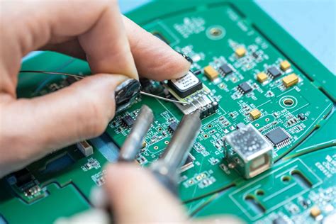
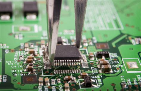
The manufacturing process itself introduces further complexities.
Flex PCB antennas are typically produced using photolithography, a process that involves transferring a pattern onto a substrate using light. This process must be executed with extreme precision to ensure that the intricate patterns required for NFC antennas are accurately reproduced. Any deviation can result in defects that affect the antenna’s performance. Moreover, the process must be scalable to meet the high-volume demands of the market, which requires careful optimization of each step to maintain quality while increasing throughput.
Despite these challenges, several solutions have been developed to enhance the manufacturing of NFC flex PCB antennas.
Advances in material science have led to the development of new conductive inks and substrates that offer improved flexibility and durability. These materials can be printed using advanced techniques such as inkjet or screen printing, which allow for greater design flexibility and reduced production costs. Additionally, the use of computer-aided design (CAD) tools has revolutionized the design process, enabling more accurate simulations and faster iterations.
Furthermore, innovations in manufacturing technology, such as roll-to-roll processing, have significantly increased production efficiency.
This method allows for continuous production of flex PCBs, reducing waste and lowering costs. Quality control has also been enhanced through the use of automated inspection systems that can quickly identify defects and ensure that each antenna meets stringent performance standards.
In conclusion, while the manufacturing of NFC flex PCB antennas presents numerous challenges, ongoing advancements in materials, design, and production technologies offer promising solutions. These innovations not only address current manufacturing hurdles but also pave the way for future developments in NFC technology, ensuring that it remains a vital component of the ever-evolving landscape of wireless communication.
Future Trends in NFC Flex PCB Antenna Technology
The evolution of Near Field Communication (NFC) technology has been remarkable, with its applications expanding across various industries, from contactless payments to smart home devices. At the heart of this technology lies the NFC flex PCB antenna, a critical component that facilitates seamless communication between devices. As we look to the future, several trends are poised to shape the development and deployment of NFC flex PCB antennas, promising to enhance their functionality and integration capabilities.
To begin with, the miniaturization of electronic components continues to be a driving force in the advancement of NFC flex PCB antennas.
As consumer electronics become increasingly compact, there is a growing demand for smaller, more efficient antennas that can be integrated into limited spaces without compromising performance. This trend is pushing manufacturers to innovate in the design and materials used in flex PCBs, enabling the creation of antennas that are not only smaller but also more flexible and durable. Consequently, this miniaturization is expected to open new avenues for NFC applications in wearable technology and other compact devices.
In addition to miniaturization, the integration of advanced materials is another trend that is set to revolutionize NFC flex PCB antennas.
Researchers are exploring the use of novel materials such as graphene and other conductive polymers, which offer superior electrical properties and flexibility compared to traditional materials. These advanced materials have the potential to significantly enhance the performance of NFC antennas, providing higher data transfer rates and improved signal strength. As these materials become more commercially viable, they are likely to be adopted widely, leading to more efficient and reliable NFC communication.
Moreover, the rise of the Internet of Things (IoT) is expected to further drive the demand for NFC flex PCB antennas.
As IoT devices proliferate, there is an increasing need for efficient communication protocols that can support a vast network of interconnected devices. NFC technology, with its low power consumption and secure data transfer capabilities, is well-suited to meet these requirements. Consequently, the development of NFC flex PCB antennas that can seamlessly integrate with IoT devices is anticipated to be a key focus area for manufacturers. This integration will likely facilitate the creation of smarter, more connected environments, enhancing the overall user experience.
Furthermore, sustainability is becoming an increasingly important consideration in the development of electronic components, including NFC flex PCB antennas.
As environmental concerns continue to mount, there is a growing emphasis on creating sustainable and eco-friendly products. This trend is prompting manufacturers to explore recyclable materials and energy-efficient production processes in the design of NFC antennas. By prioritizing sustainability, the industry aims to reduce its environmental footprint while meeting the evolving demands of consumers and regulatory bodies.
In conclusion, the future of NFC flex PCB antenna technology is set to be shaped by several key trends, including miniaturization, the integration of advanced materials, the rise of IoT, and a focus on sustainability. These trends are expected to drive innovation and enhance the capabilities of NFC antennas, enabling them to meet the growing demands of modern technology. As these developments unfold, NFC flex PCB antennas will likely play an increasingly vital role in facilitating seamless communication across a wide range of applications, paving the way for a more connected and efficient future.