Optimization Methods for Dense Solder Joints in PCB Design
Abstract
With the continuous miniaturization of electronic devices and the increasing complexity of circuit designs, printed circuit board (PCB) layouts often face challenges related to dense solder joints. Overly close solder joints can lead to issues such as solder bridging, short circuits, and reduced reliability. This paper explores various optimization techniques to address high-density solder joints in PCB design, including pad design, solder mask application, component placement, routing strategies, and manufacturing considerations. By implementing these methods, designers can improve solder joint quality, enhance manufacturability, and ensure long-term reliability.
1. Introduction
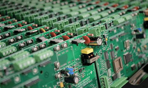
Modern PCB designs must accommodate higher component densities while maintaining manufacturing feasibility and reliability. One of the critical challenges is managing densely packed solder joints, particularly in fine-pitch components such as ball grid arrays (BGAs), quad flat packages (QFPs), and chip-scale packages (CSPs). Excessive solder joint density increases the risk of defects during assembly, including bridging, insufficient solder, and tombstoning.
This paper discusses several optimization approaches to mitigate these risks, focusing on design modifications, material selection, and manufacturing techniques.
2. Pad Design Optimization
2.1. Pad Size and Shape Adjustment
- Reducing Pad Size: For fine-pitch components, reducing pad dimensions can increase the spacing between adjacent solder joints without altering the component footprint. However, excessively small pads may weaken mechanical strength.
- Non-Standard Pad Shapes: Using oval, rectangular, or custom-shaped pads instead of circular ones can improve clearance in tight spaces.
2.2. Solder Mask Defined (SMD) vs. Non-Solder Mask Defined (NSMD) Pads
- SMD Pads: The solder mask covers part of the copper pad, reducing the exposed area and minimizing solder spreading. This approach is beneficial for preventing bridging.
- NSMD Pads: The entire copper pad is exposed, providing better mechanical strength but increasing the risk of solder bridging in dense layouts.
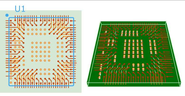
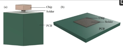
2.3. Via-in-Pad and Microvia Techniques
- Via-in-Pad: Placing vias directly within component pads saves space but requires careful filling and planarization to avoid solder wicking.
- Laser Microvias: These allow high-density interconnections without occupying excessive board space, reducing the need for closely spaced through-hole vias.
3. Solder Mask and Surface Finish Considerations
3.1. Solder Mask Application
- Precision Solder Mask Alignment: Ensuring accurate solder mask registration prevents mask slivers between pads, which can lead to bridging.
- Solder Mask Expansion: Adjusting the solder mask expansion (the overlap between mask and pad) can help control solder flow.
3.2. Surface Finishes
- Electroless Nickel Immersion Gold (ENIG): Provides a flat surface, improving solder joint definition.
- Organic Solderability Preservative (OSP): A cost-effective option but may require tighter process control.
- Immersion Silver or Tin: Alternative finishes that can enhance solderability in dense layouts.
4. Component Placement and Routing Strategies
4.1. Strategic Component Arrangement
- Avoiding Clustering High-Density Components: Distributing fine-pitch components across the PCB reduces localized solder joint congestion.
- Orientation Alignment: Aligning components in the same direction simplifies soldering and reduces bridging risks.
4.2. Trace Routing Techniques
- Thinner Traces with Adequate Spacing: Using narrower traces with proper clearance helps prevent unintended solder connections.
- Escape Routing for BGAs: Employing dog-bone or via-in-pad techniques for BGA breakout routing optimizes space usage.
5. Manufacturing Process Adjustments
5.1. Stencil Design for Solder Paste Application
- Reduced Aperture Size: Smaller stencil apertures limit solder paste volume, decreasing the chance of bridging.
- Step Stencils: Using varying stencil thicknesses helps control paste deposition for different pad sizes.
5.2. Reflow Profile Optimization
- Controlled Ramp Rates: Prevents excessive solder spreading before reflow.
- Peak Temperature Management: Ensures proper solder melting without causing excessive wetting.
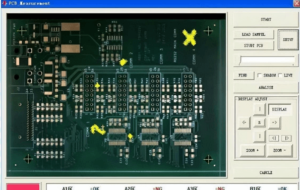
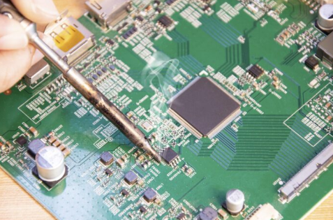
5.3. Inspection and Rework Techniques
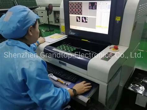
- Automated Optical Inspection (AOI): Detects solder bridging and insufficient joints early.
- Selective Laser Rework: Allows precise correction of defective solder joints in dense areas.
6. Advanced Techniques for High-Density PCBs
6.1. Embedded Components
- Integrating passive components within the PCB layers reduces surface-mounted joint density.
6.2. 3D Printing and Additive Manufacturing
- Enables innovative PCB structures with optimized solder joint distribution.
6.3. Flexible and Rigid-Flex PCBs
- Distributing components across multiple rigid and flexible sections can alleviate joint density issues.
7. Conclusion
Optimizing PCB designs with dense solder joints requires a multi-faceted approach, combining careful pad design, solder mask application, component placement, and manufacturing adjustments. By implementing these strategies, designers can mitigate soldering defects, enhance reliability, and support the ongoing trend toward miniaturization in electronics. Future advancements in materials and manufacturing techniques will further improve high-density PCB assembly.