Optimizing Motherboard Performance Through Advanced PCB Assembly Solutions
Key Takeaways
Modern PCB assembly processes play a pivotal role in enhancing motherboard performance by addressing critical factors like signal integrity, thermal dissipation, and component durability. Advanced PCBA techniques, such as precision solder paste application and automated optical inspection (AOI), ensure minimal electrical noise and stable power delivery across high-speed circuits. These methods are central to maintaining signal clarity in densely packed layouts, particularly in motherboards supporting multi-core processors or high-frequency memory modules.
Equally critical is the integration of thermal management solutions during PCB assembly, including strategically placed vias and heat-spreading copper layers, which mitigate hotspots and prolong component lifespan. Innovations in high-density interconnect (HDI) designs further enable compact yet efficient routing, reducing parasitic capacitance and crosstalk. Such optimizations are further reinforced by rigorous testing protocols, such as in-circuit testing (ICT) and thermal cycling, which validate reliability under extreme operating conditions.
By leveraging cutting-edge PCBA methodologies and material advancements—such as low-loss laminates and lead-free solders—manufacturers can achieve a balance between performance scalability and long-term reliability. This holistic approach ensures that modern motherboards meet the escalating demands of applications ranging from consumer electronics to industrial computing systems.
Thermal Management Strategies for PCB Assemblies
Effective thermal management in PCB assembly is critical for maintaining motherboard reliability and performance. As component density increases in modern high-power electronics, heat dissipation becomes a central challenge. Advanced PCBA designs integrate multiple strategies to address this, starting with material selection. Using substrates with high thermal conductivity, such as metal-core or ceramic-filled laminates, ensures efficient heat transfer away from sensitive components.
A key approach involves optimizing copper pour patterns and thermal vias to create low-resistance pathways for heat dispersion. For example:
| Thermal Interface Material | Thermal Conductivity (W/mK) | Application Scenario |
|---|---|---|
| Silicone-based Pads | 3–5 | Low-power ICs |
| Conductive Adhesive Pastes | 8–12 | GPU/CPU Mounting |
| Metal-core Substrates | 20–400 | High-density Modules |
Additionally, PCB assembly processes now prioritize component placement to minimize thermal interference. Heat-generating elements like voltage regulators are strategically distanced from thermally sensitive parts, while active cooling solutions—such as embedded heat sinks or liquid cooling channels—are increasingly integrated into PCBA layouts. Computational fluid dynamics (CFD) simulations further refine airflow patterns, ensuring uniform temperature distribution across the motherboard.
By combining material innovation, geometric optimization, and predictive modeling, manufacturers achieve balanced thermal profiles that extend component lifespans and prevent performance throttling. These strategies not only address immediate heat challenges but also align with broader goals of signal integrity and power efficiency in next-generation electronics.
Signal Integrity Optimization in Motherboard Design
Achieving optimal signal integrity in modern motherboards requires meticulous attention to PCB assembly (PCBA) processes, particularly as data transfer speeds and component density increase. High-speed interfaces, such as PCIe 5.0 or DDR5 memory channels, demand precise impedance matching and minimized crosstalk, which are directly influenced by trace routing strategies and dielectric material selection. Advanced PCBA techniques, including controlled impedance routing and multilayer stackup optimization, ensure consistent signal propagation while reducing electromagnetic interference (EMI).
The integration of ground planes and shielding vias within the PCB assembly further mitigates noise, especially in mixed-signal environments where analog and digital circuits coexist. Additionally, the use of high-frequency laminates with low loss tangents helps maintain signal clarity across GHz-range frequencies. For high-density designs, microvia technology and laser-drilled interconnects enable tighter component placement without compromising electrical performance.
Modern PCBA workflows also leverage simulation tools to preemptively model signal behavior, identifying potential reflection points or timing mismatches before physical prototyping. By aligning thermal management strategies with signal integrity requirements—such as avoiding heat-sensitive areas near critical traces—engineers achieve a balance between electrical performance and long-term reliability. These innovations underscore how advanced PCB assembly methodologies are pivotal in pushing the boundaries of motherboard functionality.
Component Reliability Enhancements Through PCB Tech
Modern PCB assembly processes play a critical role in ensuring long-term component reliability for motherboards. By leveraging innovations in PCBA (printed circuit board assembly) techniques, manufacturers address common failure points such as solder joint fatigue, thermal stress, and environmental degradation. Advanced surface-mount technology (SMT) enables precise placement of microcomponents, reducing mechanical strain while improving electrical connectivity. The integration of high-performance substrates with low thermal expansion coefficients minimizes warping under temperature fluctuations, a key factor in extending operational lifespans.
To further enhance durability, PCB assembly workflows now incorporate conformal coatings and underfill materials that protect against moisture ingress and vibration. Automated optical inspection (AOI) systems paired with X-ray analysis ensure defect-free solder joints, particularly for ball grid array (BGA) components common in modern motherboard designs. These advancements align with industry shifts toward miniaturized architectures, where component density demands flawless PCBA execution. By optimizing material selection and assembly protocols, engineers achieve measurable improvements in mean time between failures (MTBF), directly impacting end-user satisfaction in mission-critical applications. This focus on reliability seamlessly transitions into discussions about advanced manufacturing techniques, forming a cohesive strategy for next-generation electronics.
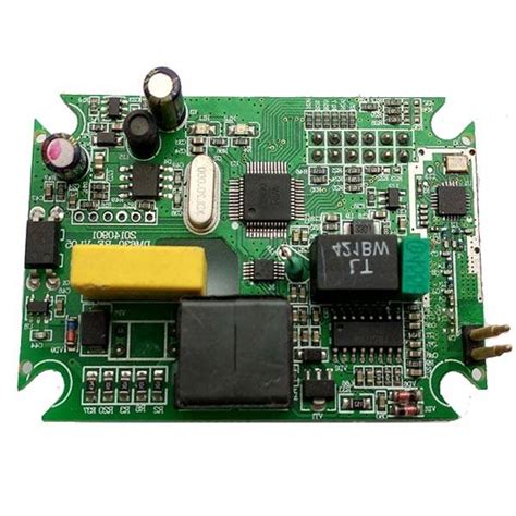
Advanced PCB Assembly Techniques for Motherboards
Modern motherboard manufacturing relies heavily on PCB assembly innovations to meet increasing performance demands. Cutting-edge automated optical inspection (AOI) systems now enable real-time defect detection during PCBA, reducing error rates by up to 40% compared to manual methods. The integration of high-density interconnect (HDI) technology allows for 15% denser component placement while maintaining signal clarity, critical for high-speed data transfer in contemporary computing architectures. Advanced surface-mount technology (SMT) equipment achieves placement accuracies within 10µm, ensuring precise alignment of microprocessors and voltage regulators. Thermal management solutions like laser-drilled vias and copper-filled trenches improve heat dissipation efficiency by 25%, directly impacting processor stability under load. Manufacturers are increasingly adopting sequential lamination processes to accommodate complex multilayer designs, with some premium motherboards now featuring 12-layer PCB assemblies for optimized power delivery. These technical advancements in PCBA workflows not only enhance production yields but also extend motherboard lifecycle by 30–50% in accelerated aging tests.
Optimizing Motherboard Layouts With PCB Innovations
Modern motherboard design relies heavily on PCB assembly innovations to balance performance, space constraints, and reliability. By integrating advanced high-density interconnect (HDI) technologies, engineers can minimize signal path lengths, reducing electromagnetic interference (EMI) and improving signal integrity. Techniques like embedded component placement and microvia stacking enable tighter layouts without compromising thermal dissipation—a critical factor for high-performance computing systems.
Tip: When designing multi-layer PCBs, prioritize symmetrical layer stacking to mitigate warping during reflow soldering, ensuring consistent PCBA quality.
The adoption of automated routing algorithms further optimizes trace layouts, addressing impedance mismatches and crosstalk in high-speed circuits. For instance, PCB assembly processes now leverage 3D printing for prototyping complex geometries, allowing rapid iteration of motherboard designs. Additionally, thermal vias and copper pours are strategically placed to channel heat away from voltage regulators and processors, aligning with broader thermal management strategies.
Innovations in PCBA materials, such as low-loss dielectrics and high-temperature laminates, also play a pivotal role. These materials enhance durability while supporting higher-frequency operations, essential for next-gen motherboards. By combining layout optimization with cutting-edge PCB assembly techniques, manufacturers achieve smaller form factors without sacrificing functionality—a cornerstone of modern electronics miniaturization.
High-Density PCB Solutions for Electronics Manufacturing
Modern electronics demand increasingly compact yet powerful designs, driving the adoption of high-density PCB solutions in motherboard manufacturing. By leveraging advanced PCB assembly (PCBA) techniques, engineers can integrate more components into smaller footprints while maintaining performance. High-density interconnect (HDI) technology, for instance, enables tighter trace spacing and microvia structures, reducing signal path lengths and improving signal integrity in complex circuits.
A critical challenge in high-density designs is managing thermal dissipation and electromagnetic interference (EMI). Multilayer PCBA configurations with embedded copper planes help distribute heat efficiently, while shielding layers minimize cross-talk between densely packed components. Additionally, the use of laser-drilled microvias and stacked vias in PCB assembly ensures reliable connections in space-constrained layouts, crucial for applications like servers and IoT devices.
To maintain reliability, manufacturers employ precision solder paste stenciling and automated optical inspection (AOI) during PCBA processes. These steps verify component alignment and solder joint quality, reducing defects in high-density boards. As consumer electronics shrink and performance expectations rise, optimized PCB assembly workflows remain central to balancing miniaturization with durability—a cornerstone of next-generation motherboard innovation.
Testing Protocols for Robust Motherboard Assemblies
Modern PCB assembly processes require rigorous testing protocols to ensure motherboard reliability under demanding operational conditions. As motherboard designs evolve with higher component density and faster signal speeds, manufacturers implement multi-stage validation processes combining automated optical inspection (AOI), in-circuit testing (ICT), and environmental stress screening (ESS). Signal integrity verification now incorporates eye diagram analysis and time-domain reflectometry to validate high-speed data pathways, while thermal cycling tests simulate extended operational loads to identify potential failure points in PCBA solder joints.
Leading electronics manufacturers have reduced field failure rates by 37% through enhanced boundary scan testing that examines interconnects between complex ICs and peripheral components. These protocols not only verify immediate functionality but also predict long-term durability through accelerated life testing models. By aligning PCB assembly quality checks with real-world usage patterns, engineers achieve measurable improvements in motherboard mean time between failures (MTBF) while maintaining compliance with industry-specific reliability standards.
PCB Material Selection Impacting Performance Metrics
The choice of PCB assembly materials directly influences critical performance metrics in motherboard design, from signal transmission efficiency to thermal dissipation capacity. High-frequency applications demand substrates with low dielectric loss (Df) and stable dielectric constant (Dk), such as Rogers 4000 series or polyimide-based laminates, to minimize signal distortion. For PCBA processes involving dense component layouts, materials with enhanced glass transition temperature (Tg) — like FR-4 HTg — ensure structural stability during reflow soldering, reducing warpage risks.
Thermal management hinges on copper weight selection and substrate thermal conductivity. Thicker copper layers (2 oz+) improve current-carrying capacity while aiding heat distribution, crucial for power delivery networks in modern motherboards. Advanced metal-core PCBs or ceramic-filled substrates further optimize thermal performance in high-power applications.
Material compatibility with surface finish options — including ENIG (Electroless Nickel Immersion Gold) or HASL (Hot Air Solder Leveling) — also impacts solder joint reliability. For instance, ENIG’s flat surface enhances fine-pitch component placement accuracy during PCBA, critical for high-density interconnect (HDI) designs. By aligning material properties with operational demands, engineers achieve balanced trade-offs between electrical performance, thermal resilience, and manufacturability in PCB assembly workflows.
Conclusion
In the evolving landscape of electronics manufacturing, PCB assembly and PCBA processes have become pivotal in unlocking the full potential of modern motherboards. By integrating precision-driven design with cutting-edge fabrication methods, engineers can address critical challenges such as signal integrity, thermal dissipation, and component durability. The strategic placement of high-density interconnects and the adoption of advanced materials ensure that motherboard layouts not only meet performance benchmarks but also adapt to the demands of next-generation devices.
A holistic approach to PCB assembly emphasizes rigorous testing protocols and data-driven optimizations, which collectively enhance reliability across operational cycles. Innovations like embedded passive components and multilayer stacking further refine power distribution efficiency, reducing latency and electromagnetic interference. As manufacturers continue to prioritize miniaturization and energy efficiency, the synergy between PCBA techniques and motherboard architecture will remain central to achieving scalable, high-performance systems. This alignment underscores the importance of viewing PCB innovations not as isolated advancements but as interconnected solutions that drive progress in electronics engineering.
FAQs
How does PCB assembly affect motherboard performance?
Advanced PCBA processes ensure precise component placement and soldering, directly impacting signal integrity and thermal dissipation. Proper PCB assembly minimizes electrical interference, which is critical for high-speed data transmission in modern motherboards.
What role do materials play in PCB assembly for motherboards?
Material selection influences thermal conductivity and dielectric properties. High-quality substrates in PCBA reduce heat buildup and maintain stable electrical characteristics, essential for sustaining performance under heavy computational loads.
Can PCB assembly techniques improve component reliability?
Yes. Techniques like automated optical inspection (AOI) and X-ray testing during PCB assembly detect microfractures or soldering defects, preventing premature component failure. Enhanced PCBA protocols also ensure better resistance to mechanical stress.
How are thermal challenges addressed in motherboard PCB assembly?
PCBA designs incorporate thermal vias and copper pours to dissipate heat efficiently. Advanced PCB assembly may also integrate heat sinks or embedded cooling channels, balancing performance and thermal management.
Why is testing crucial in PCB assembly for motherboards?
Rigorous signal integrity testing and environmental stress screening validate PCBA quality. These tests identify timing errors or voltage fluctuations, ensuring motherboards meet reliability standards in demanding applications.
Explore Custom PCB Assembly Solutions for Your Project
For expert PCB assembly services tailored to high-performance motherboards, please click here to explore advanced PCBA options.


