Panasonic Megtron 6 Datasheet: Low Dk and H-VLP Material Data
Key Takeaways
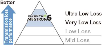
When selecting materials for PCB manufacturing, understanding the balance between performance and PCB manufacturing cost is critical. Panasonic Megtron 6’s datasheet highlights ultra-low loss characteristics, driven by its Low Dk glass cloth and H-VLP copper foil, which directly address signal integrity challenges in high-speed designs. For PCB manufacturing companies, these properties reduce the need for complex compensation techniques, simplifying production workflows.
The 0.75mm sample thickness offers a practical starting point for prototyping, allowing engineers to validate designs before scaling to mass production—a key advantage for optimizing PCB manufacturing business efficiency. Additionally, the material’s thermal stability ensures consistent performance across temperature fluctuations, reducing risks in demanding applications like automotive or data centers.
Below is a comparison of Megtron 6’s critical parameters for PCB manufacturing applications:
| Parameter | Megtron 6 Specification | Industry Standard |
|---|---|---|
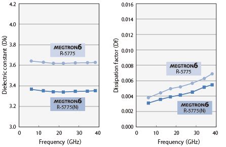
| Dk @ 10 GHz | 3.7 | 4.2–4.5 |
| Dissipation Factor (Df) | 0.0015 | 0.002–0.003 |
| Thermal Decomposition | >340°C | 280–320°C |
By prioritizing HDI design optimization and leveraging these specifications, PCB manufacturing companies can achieve tighter impedance control and minimize layer counts, further lowering PCB manufacturing cost while maintaining reliability. This positions the material as a strategic choice for businesses aiming to compete in high-frequency markets.
Panasonic Megtron 6 Datasheet Key Specs
When evaluating materials for high-frequency applications, the Panasonic Megtron 6 datasheet provides critical insights into its performance benchmarks. Key specifications include a low dielectric constant (Dk) of 3.2 at 10 GHz and a dissipation factor (Df) below 0.0015, making it ideal for minimizing signal loss in PCB manufacturing for 5G or high-speed computing. The combination of Low Dk glass cloth and H-VLP copper foil ensures consistent impedance control, which is vital for reducing PCB manufacturing cost by minimizing rework during prototyping.
For PCB manufacturing companies, the material’s thermal stability (Tg > 180°C) and low CTE (12 ppm/°C) translate to reliable performance under thermal stress, reducing long-term failure risks. The datasheet also highlights 0.75mm thickness options, enabling compact HDI designs without sacrificing signal integrity—a crucial factor for optimizing PCB manufacturing business workflows.
Tip: Always cross-reference the datasheet’s typical data—like insertion loss curves and thermal aging results—with your application’s operating conditions to avoid over-engineering.
For detailed material property charts or to request samples, consult Panasonic’s official documentation. By aligning these specs with your design goals, you can balance performance and PCB manufacturing cost while meeting stringent industry standards.
Low Dk Glass Cloth Material Analysis
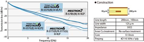
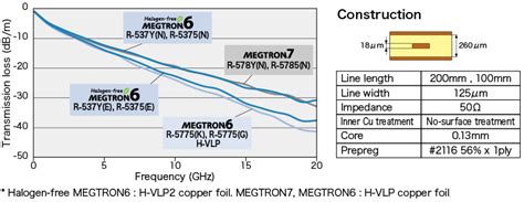
When selecting materials for high-speed PCB manufacturing, the dielectric constant (Dk) of the substrate plays a critical role in signal integrity. Panasonic Megtron 6’s low Dk glass cloth reduces signal distortion by maintaining consistent electrical properties across frequencies, making it ideal for applications requiring ultra-low loss performance. For PCB manufacturing companies, this material’s stability translates to reduced impedance variations, particularly in multilayer designs where layer-to-layer alignment is paramount.
The glass cloth’s composition also minimizes dispersion effects, ensuring reliable data transmission even at frequencies above 10 GHz. This characteristic directly impacts PCB manufacturing cost by lowering the need for error-prone compensation techniques during fabrication. Additionally, the material’s thermal expansion properties align closely with copper, reducing stress-induced failures in high-temperature environments—a key consideration for PCB manufacturing business models focused on reliability-driven markets.
By integrating low Dk glass cloth, designers achieve tighter impedance control while optimizing stackup configurations. This compatibility with H-VLP copper foil further enhances high-frequency performance, creating a synergistic effect that simplifies design validation cycles. For applications demanding precision, such as 5G infrastructure or advanced computing, this material combination ensures consistent results without compromising manufacturability.
H-VLP Copper Foil Technical Insights
When designing high-speed PCBs, the choice of copper foil directly impacts signal integrity and manufacturing efficiency. Panasonic’s Megtron 6 leverages H-VLP (Hyper Very Low Profile) copper foil, a critical innovation for minimizing insertion loss in high-frequency applications. Unlike standard foils, H-VLP’s ultra-smooth surface reduces roughness-induced attenuation, ensuring consistent impedance control even in densely routed designs. For PCB manufacturing companies, this translates to improved yield rates and lower PCB manufacturing cost, as fewer retries are needed to meet stringent signal integrity requirements.
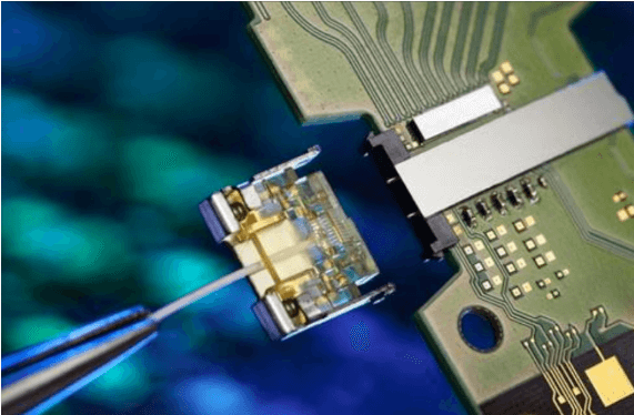
The bonding strength between H-VLP copper and Megtron 6’s low-Dk glass cloth ensures reliability under thermal stress, a key consideration for PCB manufacturing business models prioritizing long-term performance. Additionally, the foil’s thin profile (typically ≤ 3µm) supports HDI (High-Density Interconnect) designs, enabling finer traces and microvias without compromising mechanical stability. When evaluating PCB manufacturing options, verify that suppliers can handle H-VLP’s precise lamination requirements—improper processing can negate its performance advantages. By integrating this material, you achieve a balance between ultra-low loss characteristics and scalable production, critical for next-gen applications like 5G infrastructure or high-speed computing.
Another critical factor is H-VLP’s compatibility with lead-free assembly processes, which aligns with global sustainability mandates. This adaptability ensures that your PCB manufacturing workflows remain future-proof, even as regulatory standards evolve.
0.75mm Sample Thickness Applications
When designing high-speed circuits, the PCB manufacturing process demands precise material selection to balance performance and practicality. Panasonic Megtron 6’s 0.75mm sample thickness offers a critical advantage for applications requiring high-density interconnects (HDIs) or constrained spatial layouts. This optimized thickness enables PCB manufacturing companies to achieve tighter layer stacking while maintaining signal integrity—a necessity for advanced RF systems or millimeter-wave devices.
The 0.75mm profile supports impedance control in multi-layered boards, reducing the risk of signal distortion even in compact designs. For cost-sensitive projects, this thickness minimizes PCB manufacturing cost by lowering material waste and simplifying lamination cycles. Its compatibility with H-VLP copper foil further enhances high-frequency performance, ensuring stable dielectric properties under thermal stress—a key factor for automotive or aerospace electronics.
For PCB manufacturing business strategies, offering Megtron 6 as a standard material option can differentiate your services in competitive markets. The 0.75mm variant’s thermal stability and ultra-low loss characteristics align with evolving industry standards, making it ideal for 5G infrastructure or AI-driven hardware. When implementing this thickness, prioritize design simulations to validate insertion loss and cross-talk thresholds, ensuring end-use reliability without compromising fabrication efficiency.
Ultra-Low Loss Circuit Performance
When designing high-speed circuits, minimizing signal loss becomes critical for maintaining signal integrity, especially in applications like 5G infrastructure or advanced computing systems. Panasonic Megtron 6 addresses this challenge through its ultra-low dissipation factor (Df), which reduces energy absorption at high frequencies. By combining low Dk glass cloth with H-VLP copper foil, the material ensures consistent impedance control, even in multi-layered designs. This performance advantage directly impacts PCB manufacturing costs, as fewer design iterations are needed to compensate for signal degradation.
For PCB manufacturing companies, leveraging Megtron 6’s properties translates to improved yield rates in high-frequency applications. Its optimized dielectric properties reduce insertion loss by up to 20% compared to standard FR-4 materials, enabling thinner traces without sacrificing performance. This is particularly valuable for PCB manufacturing businesses focused on compact, high-density interconnects (HDIs), where space constraints demand precision. Additionally, the material’s thermal stability minimizes phase shifts over temperature fluctuations, ensuring reliability in environments like automotive radar or data centers.
By integrating Megtron 6 into your stack-up, you gain access to datasheet-validated parameters that simplify simulation and prototyping. This reduces time-to-market for high-speed designs while aligning with cost-sensitive PCB manufacturing strategies. The 0.75mm sample thickness further allows testing across varied use cases, from RF modules to server backplanes, without compromising signal fidelity.

HDI Design Optimization Strategies
When implementing HDI design optimization strategies with Panasonic Megtron 6, you need to balance signal integrity with PCB manufacturing cost efficiencies. The material’s ultra-low loss characteristics enable tighter trace spacing without compromising performance, critical for high-density layouts in advanced applications. By leveraging Megtron 6’s Low Dk glass cloth and H-VLP copper foil, you reduce parasitic capacitance and impedance mismatches, which simplifies impedance control in multilayer designs.
For PCB manufacturing companies, the 0.75mm sample thickness offers flexibility in creating microvias and stacked structures, minimizing layer counts while maintaining thermal stability. This directly impacts PCB manufacturing business profitability by reducing material waste and processing steps. To further optimize costs, pair the material’s low dissipation factor with laser-drilled microvias, ensuring reliable interconnects even in ultra-thin substrates.
Transitioning from traditional FR-4 to Megtron 6 requires adjusting lamination parameters and via fill techniques. Collaborate with fabricators to validate thermal expansion coefficients and glass transition temperatures, ensuring compatibility with high-speed signal requirements. By integrating these strategies, you achieve a scalable solution that aligns with both performance benchmarks and PCB manufacturing budget constraints.
Thermal Stability in High-Speed PCBs
When designing high-speed circuits, maintaining thermal stability becomes critical to prevent performance degradation under operational stress. Panasonic Megtron 6 addresses this challenge through its low thermal expansion properties and optimized resin systems, which minimize dimensional shifts even at elevated temperatures. For PCB manufacturing companies, this translates to reduced warpage risks during lamination and reflow processes, directly lowering PCB manufacturing cost by minimizing material waste and rework.
The material’s glass transition temperature (Tg) of 180°C ensures reliability in environments where heat buildup is inevitable, such as in 5G infrastructure or high-power computing modules. This stability also supports HDI design optimization, enabling tighter via spacing without compromising structural integrity. For businesses focused on PCB manufacturing business scalability, Megtron 6’s consistent performance across temperature cycles extends product lifespans, reducing long-term maintenance expenses.
By integrating Megtron 6 into your stack-up, you ensure signal integrity remains intact even during thermal cycling, a key requirement for applications like automotive radar or data center servers. This reliability aligns with the demands of high-volume PCB manufacturing, where material consistency directly impacts yield rates and client satisfaction.
Typical Data for Megtron 6 Materials
When evaluating materials for PCB manufacturing, Panasonic Megtron 6’s datasheet provides critical insights into performance benchmarks. Key metrics include Dk (dielectric constant) values as low as 3.2 at 10 GHz and Df (dissipation factor) below 0.0015, ensuring minimal signal loss in high-frequency designs. These properties make it ideal for PCB manufacturing companies targeting 5G infrastructure or advanced computing systems.
The material’s H-VLP copper foil further enhances performance, with surface roughness reduced to ≤1.5 μm, minimizing conductor losses. For PCB manufacturing cost optimization, the 0.75mm thickness option balances mechanical stability with space efficiency, enabling compact HDI design without compromising thermal resilience. Thermal stability data—such as a glass transition temperature (Tg) exceeding 180°C and thermal expansion rates below 2.5%—ensures reliability under high-speed operating conditions, a critical factor for PCB manufacturing business clients prioritizing long-term durability.
Transitioning from material properties to real-world application, this data helps engineers predict how Megtron 6 performs under varying frequencies and temperatures. For example, insertion loss remains under -0.15 dB/inch at 28 GHz, aligning with requirements for next-gen RF applications. By integrating these specifications early in the design phase, PCB manufacturing teams can avoid costly revisions while meeting stringent performance targets.
Request Megtron 6 Sample Information
When evaluating materials for PCB manufacturing, access to physical samples is critical to validate performance claims. For PCB manufacturing companies considering Panasonic Megtron 6, requesting sample kits provides hands-on insights into its low Dk glass cloth and H-VLP copper foil characteristics. These samples, typically offered in 0.75mm thickness, allow engineers to test ultra-low loss properties under real-world conditions, such as high-frequency signal integrity or thermal cycling scenarios.
To streamline your assessment, Panasonic’s sample program includes typical data sheets that align with PCB manufacturing cost calculations, helping you compare material efficiency against alternative substrates. For instance, testing the thermal stability of Megtron 6 can reveal long-term reliability advantages, directly impacting PCB manufacturing business decisions like warranty terms or maintenance schedules. When requesting samples, specify application requirements (e.g., layer count, operating frequency) to ensure the provided materials match your design parameters.
Transitioning from prototypes to full-scale production becomes smoother when material behavior is verified early. By leveraging sample data, you can optimize HDI design strategies and minimize post-production revisions—a key consideration for balancing performance and PCB manufacturing cost. Ensure your supplier provides complete technical support during this phase, including guidance on lamination processes or impedance control tailored to Megtron 6’s unique properties.
Conclusion
When selecting materials for high-speed applications, understanding the balance between performance and PCB manufacturing cost becomes critical. Panasonic Megtron 6’s combination of low Dk glass cloth and H-VLP copper foil provides a foundation for optimizing signal integrity while maintaining thermal stability—a key consideration for PCB manufacturing companies aiming to reduce losses in demanding environments. The 0.75mm sample thickness, paired with ultra-low loss performance, ensures compatibility with advanced HDI design strategies, enabling denser layouts without compromising reliability.
For PCB manufacturing businesses, leveraging materials like Megtron 6 can directly influence long-term project viability. Its thermal stability minimizes risks of delamination or warping during assembly, reducing rework expenses. Additionally, the availability of standardized data simplifies prototyping, allowing teams to validate designs before scaling production. Whether addressing high-frequency communication systems or power-intensive modules, integrating these materials ensures your designs meet both technical and budgetary expectations—a decisive factor in competitive PCB manufacturing markets. By aligning material choices with application-specific demands, you position projects for success without overengineering solutions.
Frequently Asked Questions
How does Megtron 6’s low Dk glass cloth benefit high-speed PCB manufacturing?
The low dielectric constant (Dk) of Megtron 6’s glass cloth reduces signal loss and delays, critical for high-frequency applications. This makes it ideal for PCB manufacturing companies designing 5G infrastructure or advanced computing systems where signal integrity is paramount.
What role does H-VLP copper play in minimizing PCB manufacturing costs?
H-VLP (Hyper Very Low Profile) copper foil ensures smoother surface roughness, lowering insertion loss. By optimizing signal transmission efficiency, it reduces the need for additional signal-boosting components, helping PCB manufacturing businesses control material and assembly expenses.
Why is the 0.75mm sample thickness significant for HDI design optimization?
The 0.75mm thickness balances mechanical stability and space efficiency, enabling compact, high-density interconnects (HDI). This is particularly valuable for applications like wearable tech or IoT devices, where PCB manufacturing demands ultra-thin yet reliable substrates.
How does thermal stability affect long-term PCB manufacturing cost efficiency?
Megtron 6’s thermal resistance minimizes warping and degradation under high temperatures, extending product lifespan. This reduces warranty claims and replacement costs, offering PCB manufacturing companies a competitive edge in reliability-focused markets.
Can Megtron 6 materials be customized for specific PCB manufacturing requirements?
Yes, Panasonic provides tailored material configurations, including variations in glass weave and resin content, to align with unique electrical or mechanical needs. Typical datasheet parameters serve as a baseline, but adjustments are possible for specialized projects.
Explore Custom PCB Manufacturing Solutions
For detailed guidance on integrating Megtron 6 into your next project, please click here to connect with experts specializing in high-performance PCB manufacturing.