PCB Assembly Best Practices for Enhanced Precision
Key Takeaways
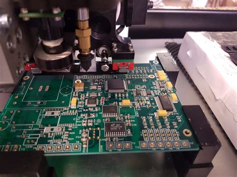
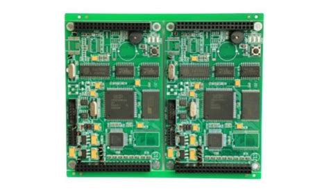
Effective PCB assembly processes for 4-layer PCBs rely on meticulous attention to component alignment, soldering precision, and inspection rigor. Achieving high-density accuracy begins with verifying component footprints against design files, ensuring thermal pad compatibility, and using automated optical alignment tools to minimize placement errors. In PCBA workflows, reflow soldering profiles must account for the thermal dissipation properties of multilayer boards, balancing peak temperatures to avoid warping while maintaining strong interlayer connections.
Third-party automated optical inspection (AOI) systems remain critical for identifying micro-scale defects, such as solder bridges or misaligned passive components, particularly in 4-layer PCB assemblies where internal vias complicate visual checks. Pairing AOI with X-ray inspection enhances reliability by validating hidden solder joints in ball grid arrays (BGAs). Additionally, maintaining ESD-safe environments and adhering to IPC-A-610 standards ensures consistent quality across production batches.
For optimal 4-layer PCB reliability, material selection plays a pivotal role. Prioritizing high-Tg substrates and low-voiding solder pastes reduces thermal stress risks during operation. By integrating these practices, manufacturers can achieve sub-10μm alignment tolerances and >99.9% first-pass yield rates, solidifying PCB assembly as a cornerstone of precision electronics manufacturing.
-Layer PCB Component Alignment Tips
Proper component alignment in 4-layer PCB assembly requires meticulous attention to mechanical and electrical design parameters. Achieving sub-10-micron placement accuracy begins with optimizing thermal expansion coefficients (TCEs) between substrates and components, particularly for high-density interconnects (HDIs). Modern PCBA workflows leverage automated optical inspection (AOI) systems with 3D solder paste detection to verify alignment before reflow soldering.
| Alignment Factor | Ideal Tolerance | Impact on Reliability |
|---|---|---|
| Component Footprint Matching | ±15 μm | Reduces solder bridging risks |
| Fiducial Marker Placement | ±25 μm | Ensures machine vision accuracy |
| Pad-to-Trace Spacing | ≥0.1 mm | Prevents signal interference |
For 4-layer PCB assembly, engineers should prioritize land pattern standardization across all layers to maintain registration consistency. Critical steps include:
- Using laser-etched fiducials with ≤0.05% positional error
- Implementing pre-reflow X-ray verification for buried vias
- Balancing copper distribution to minimize warpage during thermal cycling
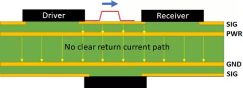
In PCBA processes, alignment errors in multilayer boards can cascade into impedance mismatches, particularly in RF sections. A 2023 IPC-6012D compliance study revealed that 62% of field failures in 4-layer designs originated from improper BGA ball grid alignment. By integrating real-time thermal profiling with pick-and-place systems, manufacturers can achieve ≤0.3° angular deviation even for 0201 chip components. This precision directly enhances signal integrity in high-speed digital circuits while reducing post-assembly rework costs by up to 40%.
Precision Soldering for 4-Layer PCBs
Achieving optimal results in PCB assembly for 4-layer boards hinges on mastering temperature-controlled soldering processes. Unlike simpler designs, 4-layer PCBs feature tighter spacing between vias and traces, demanding precise heat management to prevent delamination or warping. For PCBA workflows, using temperature-profiled reflow ovens ensures even heat distribution across all layers, critical for maintaining solder joint integrity.
Tip: Always validate thermal profiles using test coupons that mimic the actual board stack-up. This minimizes thermal stress on sensitive components like BGAs or QFNs.
When working with high-density interconnects (HDIs), prioritize low-voiding solder pastes with fine particle sizes (Type 4 or 5). These pastes reduce bridging risks in tight spaces while ensuring reliable electrical connections. For manual rework, employ micro-tip soldering irons with adjustable wattage (15–30W) to avoid overheating inner-layer copper planes. Automated optical inspection (AOI) systems should be calibrated to detect sub-0.1mm solder defects, particularly for 4-layer PCBs with buried vias.
A common pitfall in PCBA is neglecting post-soldering cooling rates. Rapid cooling can induce microcracks in joints, while overly slow cycles risk component displacement. Pairing nitrogen-assisted soldering with controlled cooling chambers enhances joint reliability, especially for boards exposed to thermal cycling in industrial applications.
By integrating these strategies, manufacturers can ensure PCB assembly processes meet the stringent demands of modern 4-layer designs, bridging precision and durability seamlessly.
Reliable PCB Assembly Inspection Protocols
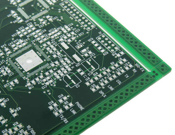
Implementing rigorous PCB assembly inspection protocols is critical for maintaining precision in 4-layer PCBA manufacturing. Automated Optical Inspection (AOI) systems provide non-destructive verification of component alignment and solder joint integrity, flagging deviations as small as 10µm. For multilayer boards, X-ray imaging becomes indispensable to inspect hidden connections like blind vias or buried traces, ensuring compliance with IPC-A-610 standards.
Post-assembly functional testing, such as In-Circuit Testing (ICT) or boundary scan, validates electrical performance by simulating operational conditions. These methods align with industry benchmarks outlined in technical documents like Yaskawa’s servo control guidelines, which emphasize tolerance thresholds for high-frequency applications. Additionally, environmental stress screening (ESS) exposes boards to thermal cycling and vibration to identify latent defects before deployment.
By integrating these protocols into 4-layer PCB assembly workflows, manufacturers reduce rework rates by up to 35% while ensuring compliance with aerospace and medical device regulations. Pairing automated systems with manual cross-checks creates a multi-tiered quality assurance framework, balancing speed and accuracy in high-volume production environments.
4-Layer PCB Assembly Best Practices
Achieving precision in 4-layer PCB assembly demands meticulous attention to design integration, process control, and material compatibility. A foundational step involves optimizing stackup symmetry to minimize warping during thermal cycles, which directly impacts PCBA reliability. Engineers should prioritize component alignment using laser-etched fiducial markers and automated optical inspection (AOI) systems, ensuring sub-10µm placement accuracy for critical ICs.
Temperature-sensitive soldering techniques, such as controlled nitrogen reflow, reduce oxidation risks in multi-layer boards while maintaining consistent joint formation. For high-density interconnects, microvia fill quality must be verified through cross-sectional analysis to prevent latent defects. Post-assembly, rigorous inspection protocols—including X-ray imaging for hidden solder bridges and automated electrical testing—are essential to validate signal integrity across all layers.
Material selection further influences precision, with low-loss laminates and high-Tg substrates recommended for stable performance under thermal stress. Implementing trace width compensation during design compensates for etching variations, preserving impedance matching in 4-layer PCBs. By integrating these practices, manufacturers can enhance yield rates and long-term reliability in complex PCB assembly projects.
Ensuring PCB Component Placement Accuracy
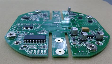
Achieving optimal PCB assembly precision begins with meticulous component placement, particularly in 4-layer PCBA designs where alignment errors can cascade across multiple signal layers. Modern automated pick-and-place systems leverage vision-assisted technology to achieve placement tolerances within ±0.025mm, critical for high-density interconnects (HDIs). For 4-layer PCBs, engineers prioritize fiducial markers as reference points, ensuring consistent alignment during both solder paste application and component mounting. Thermal profiling further minimizes placement shifts by balancing reflow oven temperatures to account for varying material expansion rates in multi-layer stacks.
To maintain accuracy, PCB assembly workflows integrate real-time feedback loops, where inline inspection systems validate component orientation and polarity before progressing to soldering stages. For fine-pitch components (e.g., BGAs or QFNs), laser-etched solder pads and vacuum-assisted nozzles prevent misalignment during high-speed placement. Additionally, adherence to IPC-A-610 standards ensures that PCBA outcomes meet industry benchmarks for mechanical and electrical reliability. By combining advanced machinery with rigorous process controls, manufacturers mitigate risks such as tombstoning or skewed components, ultimately enhancing yield rates in complex 4-layer PCB configurations.
Advanced 4-Layer PCB Reliability Methods
Achieving long-term reliability in 4-layer PCB assembly requires a strategic balance of design optimization, material science, and rigorous testing. A critical focus lies in mitigating thermal stress during PCBA processes, as uneven heat distribution across multilayer boards can lead to delamination or microcracking. Implementing controlled impedance routing ensures signal integrity in high-frequency applications, while via-in-pad techniques reduce mechanical strain on interlayer connections.
Material selection plays a pivotal role—opting for high-Tg (glass transition temperature) laminates enhances thermal stability, particularly in environments with fluctuating operating temperatures. For solder joints, low-voiding solder pastes paired with nitrogen-reflow atmospheres minimize oxidation risks, a common failure point in dense PCB assembly layouts. Post-production, accelerated life testing (ALT) simulates years of operational stress within days, identifying potential weaknesses in power distribution networks or ground plane integrity.
Advanced inspection protocols, such as 3D X-ray tomography, provide non-destructive analysis of internal layer alignment and buried vias, ensuring compliance with IPC-6012 Class 3 standards. Integrating design-for-reliability (DFR) principles early in the PCBA workflow—such as avoiding acute angles in trace routing—further fortifies multilayer boards against electromigration and fatigue. These methodologies collectively elevate the durability of 4-layer systems, aligning precision PCB assembly practices with mission-critical performance demands.
Optimizing 4-Layer Assembly Processes
Achieving precision in PCB assembly for 4-layer designs requires systematic adjustments to both design and manufacturing workflows. A key focus lies in balancing thermal management with signal integrity, particularly as PCBA complexity increases. Implementing controlled impedance routing minimizes signal distortion, while staggered via placement reduces mechanical stress during soldering cycles. For high-density boards, automated pick-and-place systems calibrated to ±0.02mm tolerance ensure component placement accuracy, especially for fine-pitch ICs and BGAs.
Another critical factor is optimizing reflow profiles for 4-layer PCBs, where variations in material thickness demand precise temperature zoning. Using nitrogen-assisted soldering chambers can mitigate oxidation risks, enhancing joint reliability. Additionally, design-for-manufacturing (DFM) checks should prioritize layer stackup symmetry to prevent warping during thermal cycling. Incorporating inline automated optical inspection (AOI) after solder paste application and post-reflow phases helps detect misalignments or insufficient solder volumes early.
Finally, collaboration between design engineers and PCBA technicians ensures thermal relief patterns and via-in-pad structures align with assembly capabilities. By refining these interconnected variables, manufacturers can reduce defect rates by up to 30% while maintaining compatibility with high-frequency and mixed-signal applications.
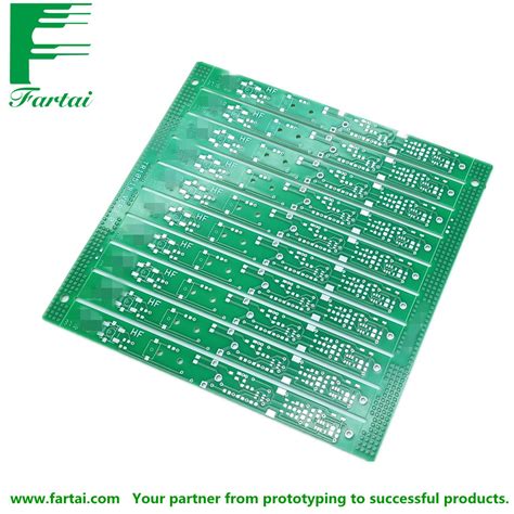
Material Selection for Enhanced PCB Precision
The foundation of precise PCB assembly begins with strategic material selection, particularly for complex 4-layer PCBA designs. Choosing substrates with stable thermal expansion coefficients ensures dimensional consistency during temperature fluctuations, reducing warping risks in multilayer configurations. High-grade FR-4 laminates with low dielectric loss are often preferred for their balance of cost and performance, while polyimide substrates excel in applications requiring extreme thermal endurance.
For conductive layers, copper foils with tightly controlled thickness tolerances (e.g., ±5%) enhance impedance matching in high-frequency circuits. When selecting solder masks, opt for liquid photoimageable (LPI) formulations that provide precise aperture definition, critical for fine-pitch component alignment. Adhesives and underfill materials must exhibit compatible glass transition temperatures (Tg) with surrounding layers to prevent delamination during thermal cycling.
A comprehensive PCB design guide emphasizes the importance of validating material datasheets against actual manufacturing capabilities. For instance, low-loss PTFE-based materials may improve signal integrity but require specialized PCBA processes for drilling and plating. Always verify solderability ratings of surface finishes like ENIG or Immersion Tin, as inconsistent wettability can compromise joint reliability in automated soldering workflows. By aligning material properties with functional requirements and production realities, engineers achieve repeatable precision across 4-layer PCB assembly batches.
Conclusion
Effective PCB assembly hinges on meticulous adherence to precision-driven practices, particularly for complex 4-layer PCBA designs. By integrating advanced alignment methodologies, controlled soldering processes, and rigorous inspection protocols, manufacturers can mitigate risks associated with signal interference and thermal imbalances. For example, verifying component placement accuracy through automated optical inspection (AOI) ensures alignment with design specifications, while reflow profiling optimizes solder joint integrity across multilayer boards.
Material selection further amplifies reliability—high-grade substrates like Hannstar MV4 94V-0 enhance dimensional stability, critical for maintaining trace tolerances in dense layouts. Post-assembly testing, including functional validation and thermal cycling, validates long-term performance under operational stressors. As PCBA technologies evolve, balancing cost-efficiency with precision remains paramount, requiring continuous refinement of assembly workflows and quality assurance frameworks. Ultimately, these practices not only elevate manufacturing consistency but also safeguard end-product functionality in demanding electronic applications.
FAQs
How does component alignment affect 4-layer PCB assembly quality?
Proper alignment ensures signal integrity and minimizes thermal stress. For PCBA projects, use automated optical inspection (AOI) systems to verify component placement accuracy, especially for high-density interconnects.
What soldering techniques enhance precision in 4-layer PCBA?
Reflow soldering with controlled thermal profiles is critical for multilayer boards. Pair this with lead-free solder alloys to maintain reliability while adhering to RoHS compliance standards.
Why are inspection protocols vital for PCB assembly reliability?
Rigorous testing, including in-circuit testing (ICT) and X-ray inspection, identifies hidden defects like voids or misalignments. These steps ensure PCBA meets performance specifications in demanding applications.
How does material selection influence 4-layer PCB precision?
High-grade substrates, such as FR-4 with low dielectric loss, improve signal stability. Pairing these with laser-drilled vias enhances layer-to-layer connectivity, reducing impedance mismatches.
Can automated systems optimize 4-layer assembly workflows?
Yes. Integrating pick-and-place machines with AOI systems streamlines production while maintaining ±0.05mm placement tolerances, crucial for advanced PCBA designs.
Ready to Elevate Your PCB Assembly Process?
For tailored solutions in high-precision PCB assembly, please click here to explore our advanced PCBA services and technical support.