PCB Conductive Via Filling Process and Its Importance
Introduction
Printed Circuit Boards (PCBs) are essential components in modern electronics, providing mechanical support and electrical connections for various electronic components. One critical aspect of PCB manufacturing is the treatment of vias—small holes drilled into the board to establish electrical connections between different layers. Among the various via treatments, conductive via filling (also known as via plugging or via-in-pad) is a crucial process that enhances PCB reliability and performance.
This article explores the conductive via filling process, its key techniques, and the reasons why it is essential in advanced PCB manufacturing.
1. What is Conductive Via Filling?
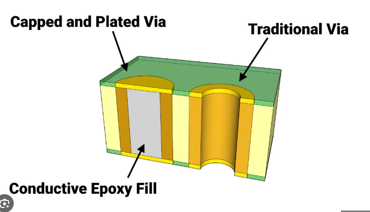
Conductive via filling refers to the process of filling plated through-holes (PTHs) or microvias with a conductive material (typically copper or silver epoxy) to ensure electrical continuity and improve mechanical stability. This technique is commonly used in high-density interconnect (HDI) PCBs, where space constraints demand efficient via utilization.
Types of Via Filling Materials
- Copper Electroplating – The most common method, where copper is electroplated inside the via to ensure conductivity.
- Conductive Epoxy (Silver or Copper-filled) – Used for smaller vias where electroplating is challenging.
- Solder Paste – Sometimes used in via-in-pad designs to improve solderability.
2. The Conductive Via Filling Process
The process involves several key steps:
Step 1: Via Drilling
- Vias are drilled using mechanical or laser drilling techniques.
- The size and depth depend on the PCB design (e.g., through-hole, blind, or buried vias).
Step 2: Desmearing and Cleaning
- After drilling, debris and resin residues (smear) are removed using chemical or plasma desmearing.
- Ensures proper adhesion of the conductive material.
Step 3: Electroless Copper Deposition
- A thin layer of copper is deposited on the via walls to establish initial conductivity.
Step 4: Electroplating (for Copper-filled Vias)
- Additional copper is electroplated to build up the conductive layer.
- Ensures low resistance and strong electrical connections.
Step 5: Via Filling
- For copper filling: Electroplating continues until the via is completely filled.
- For conductive epoxy: The epoxy is dispensed into the via and cured.
Step 6: Planarization (Surface Leveling)
- Excess material is removed to ensure a flat surface for component placement.
Step 7: Final Finishing
- Additional surface treatments (e.g., ENIG, HASL, or OSP) may be applied.
3. Reasons for Conductive Via Filling
Several factors drive the adoption of conductive via filling in PCB manufacturing:
1. Improved Electrical Performance
- Filled vias reduce impedance and signal loss, especially in high-frequency applications.
- Helps maintain signal integrity in high-speed designs (e.g., 5G, RF circuits).
2. Enhanced Thermal Management
- Filled vias improve heat dissipation by providing a thermal pathway to inner layers or heatsinks.
- Critical for power electronics and high-current PCBs.
3. Better Reliability and Durability
- Prevents air or moisture entrapment, reducing the risk of corrosion or cracking.
- Eliminates voids that could lead to mechanical failure under thermal cycling.
4. Support for Via-in-Pad Designs
- Allows vias to be placed directly under component pads, saving space in HDI PCBs.
- Ensures proper solder joint formation without solder wicking into the via.
5. Prevention of Solder Wicking
- Unfilled vias can absorb solder during reflow, leading to weak joints.
- Filled vias block solder from escaping, ensuring reliable connections.
6. Compatibility with Advanced PCB Technologies
- Essential for stacked and staggered microvias in HDI designs.
- Enables finer pitch BGA and chip-scale packaging.
4. Challenges in Conductive Via Filling
Despite its advantages, the process presents some challenges:
1. Void Formation
- Incomplete filling can leave air pockets, reducing conductivity and reliability.
- Solution: Optimized plating parameters and vacuum-assisted filling.
2. High Cost
- Electroplating and conductive epoxy increase manufacturing costs.
- Solution: Selective filling (only critical vias) to balance cost and performance.
3. Process Complexity
- Requires precise control of plating thickness and curing conditions.
- Solution: Advanced automation and inspection techniques (e.g., X-ray inspection).
5. Applications of Conductive Via Filling
- Consumer Electronics (Smartphones, Laptops) – Enables compact, high-performance PCBs.
- Automotive Electronics – Enhances reliability in harsh environments.
- Aerospace & Defense – Ensures durability under extreme conditions.
- Medical Devices – Supports miniaturized and high-reliability PCBs.
6. Future Trends in Via Filling Technology
- Laser Direct Structuring (LDS) – Allows selective via filling with high precision.
- 3D Printed Electronics – May enable new via filling methods for flexible PCBs.
- Nanomaterials – Conductive inks with nanoparticles could improve filling efficiency.
Conclusion
Conductive via filling is a critical PCB manufacturing process that enhances electrical performance, thermal management, and reliability. While it introduces additional complexity and cost, the benefits make it indispensable for modern high-density and high-frequency applications. As PCB technology evolves, advancements in materials and processes will further optimize via filling for next-generation electronics.
By understanding the process, benefits, and challenges of conductive via filling, PCB designers and manufacturers can make informed decisions to improve product quality and performance.