PCB Countersunk Holes: Design Considerations, Manufacturing Processes, and Applications
Introduction to Countersunk Holes in PCB Design
Printed Circuit Board (PCB) countersunk holes represent a specialized feature in modern electronics manufacturing that serves both functional and aesthetic purposes. These conical recesses allow screw heads to sit flush with or below the surface of the PCB, creating a smooth profile that offers numerous advantages in various applications.
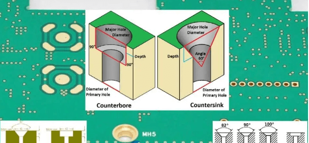
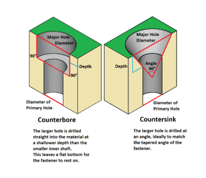
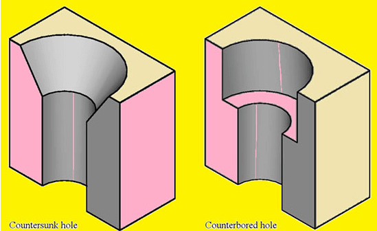
Countersunk holes differ significantly from standard through-holes in PCBs. While traditional plated through-holes maintain a cylindrical shape throughout the board’s thickness, countersunk holes feature a tapered opening at one or both surfaces of the PCB. This tapering, typically at 82°, 90°, or 100° angles, accommodates flat-head screws and creates that all-important flush mounting capability.
The evolution of countersunk holes in PCB design parallels the advancement of electronics miniaturization and the growing demand for sleek, low-profile devices. As products became thinner and more compact, traditional screw-head protrusions became increasingly problematic, driving the adoption of countersinking techniques from mechanical engineering into the realm of PCB fabrication.
Key Design Considerations for PCB Countersunk Holes
Hole Size and Angle Specifications
Designing proper countersunk holes begins with understanding the relationship between the screw size and the required hole dimensions. The countersink diameter (D) must be larger than the screw head diameter, while the angle must match the screw’s head angle—typically 82° for metric flat head screws or 90° for many standard screws.
The formula for determining the minimum countersink diameter is:
D = H + 2 × (T × tan(α/2))
Where:
- D = Countersink diameter
- H = Screw head diameter
- T = Countersink depth
- α = Countersink angle
Board Material and Thickness Constraints
The PCB material significantly impacts countersink quality. Standard FR-4, while suitable for many applications, may exhibit fiber tear-out during the countersinking process. High-Tg materials or those with reinforced glass weaves often produce cleaner countersinks. The board thickness must accommodate both the countersink depth and sufficient remaining material for structural integrity—generally, the countersink depth shouldn’t exceed 1/3 of the board thickness.
Copper Clearance and Electrical Considerations
Countersinking affects copper layers, requiring careful attention to:
- Maintaining adequate clearance between copper traces and the countersink edge
- Ensuring no copper exposure at the countersink walls that could cause short circuits
- Proper plating requirements if electrical connection through the hole is needed
Placement Relative to Board Features
Countersunk holes should be positioned:
- At least 3× the board thickness from board edges
- Away from sensitive components to avoid mechanical stress
- Considering the board’s bend radius if used in flexible applications
Manufacturing Processes for PCB Countersunk Holes
CNC Drilling Techniques
Modern PCB fabrication employs sophisticated CNC drilling machines capable of producing precise countersinks. The process typically involves:
- Initial through-hole drilling with standard drill bits
- Countersink formation using specialized tapered end mills
- Potential deburring or cleaning steps
The CNC approach offers excellent precision (±0.05mm typically achievable) and allows for programming different countersink depths across the board.
Laser Ablation Methods
For high-density or delicate boards, laser countersinking provides advantages:
- No mechanical stress on the board
- Finer control over depth and angle
- Ability to create smaller countersinks than mechanical methods
- Cleaner edges with minimal material tear-out
However, laser methods are generally slower and more expensive than mechanical drilling.
Press-Fit Countersink Technology
Some manufacturers use press-fit countersink tools that form the taper in a single operation. This method is fast but requires careful control to prevent delamination or excessive stress on the PCB layers.
Post-Processing Requirements
After countersinking, additional processes may include:
- Deburring to remove any rough edges
- Cleaning to eliminate drilling debris
- Additional plating if electrical connectivity is required
- Surface finishing application (like ENIG or HASL) that must accommodate the countersink geometry
Applications and Benefits of Countersunk Holes in PCBs
Enclosure Integration and Space Savings
The primary advantage of countersunk holes becomes evident in enclosure design:
- Allows for thinner product profiles by eliminating screw head protrusion
- Enables smooth surfaces for sliding mechanisms or mating parts
- Reduces overall assembly height in stacked configurations
Improved Aesthetics in Consumer Products
For visible electronics, countersunk screws provide:
- Cleaner, more professional appearance
- Elimination of protruding hardware that might snag or collect dirt
- Seamless integration with industrial design elements
Enhanced Mechanical Stability
Properly designed countersunk holes offer:
- Better load distribution compared to standard holes
- Reduced likelihood of screw loosening due to vibration
- More precise component alignment during assembly
Specialized Industry Applications
Countersunk PCBs find particular value in:
- Aerospace and aviation electronics where low profile is critical
- Automotive systems subject to vibration and space constraints
- Medical devices requiring smooth, cleanable surfaces
- Military equipment needing robust mechanical connections
Challenges and Limitations of PCB Countersunk Holes
Manufacturing Complexity and Cost Implications
Countersinking adds steps to the PCB fabrication process, potentially increasing:
- Tooling costs for specialized drill bits
- Machine time for additional operations
- Scrap rates due to processing challenges
Material Stress and Structural Concerns
The tapering process creates unique stresses:
- Potential for delamination near the countersink edges
- Reduced local board strength
- Risk of fiber tear-out in FR-4 materials
Plating and Coating Difficulties
Applying finishes to countersunk holes presents challenges:
- Uneven plating thickness in the tapered region
- Difficulty with solder mask application in the countersink
- Potential for pooling or unevenness in surface finishes
Tolerance Stack-Up Issues
The combination of multiple tolerances can lead to:
- Misalignment between the screw head and countersink
- Gaps or uneven seating of fasteners
- Interference with other board features
Best Practices for Implementing Countersunk Holes
Design Guidelines for Optimal Performance
- Always specify both the through-hole and countersink dimensions clearly
- Include angle tolerances (typically ±2°) in drawings
- Provide adequate keep-out zones around countersunk holes
- Consider using counterbored holes where appropriate as an alternative
Material Selection Tips
- For frequent countersinking, specify materials with tighter weave patterns
- Consider metal-core or thick-copper boards for heavy mechanical loads
- Evaluate alternative materials like polyimide for challenging applications
Drawing Callouts and Documentation
Proper documentation should include:
- Clear countersink symbols per ASME Y14.5 standards
- Complete dimensional data (diameter, angle, depth)
- Surface finish requirements
- Any special processing instructions
Prototyping and Testing Recommendations
Before full production:
- Build prototypes to verify fit with actual hardware
- Conduct mechanical stress tests
- Check for any electrical interference issues
- Validate assembly processes
Future Trends in PCB Countersunk Hole Technology
Advanced Materials Impact
Emerging PCB materials like high-performance ceramics or composite substrates may require:
- New tooling approaches for countersinking
- Alternative processing methods
- Revised design rules
Micro-Countersinking for Miniaturization
As devices shrink, we’re seeing demand for:
- Smaller diameter countersinks (below 2mm)
- Shallower angles for ultra-thin applications
- Laser-based micro-countersinking techniques
Automated Inspection Methods
Machine vision and 3D scanning technologies enable:
- In-line countersink quality verification
- Automated measurement of angle and depth
- Real-time process adjustments
Integration with Other Advanced Features
Countersinking is being combined with:
- Embedded component technology
- Advanced HDI (High Density Interconnect) designs
- Flexible and rigid-flex board constructions
Conclusion
PCB countersunk holes represent a critical intersection of mechanical and electrical design in modern electronics. When properly implemented, they provide significant advantages in product design, assembly, and performance. However, successful application requires careful consideration of design parameters, material properties, manufacturing capabilities, and end-use requirements.
As PCB technology continues to evolve, countersinking processes will likely become more refined and integrated with other advanced board features. Designers and manufacturers who master the nuances of countersunk hole implementation will be better positioned to create innovative, reliable, and aesthetically pleasing electronic products that meet the ever-increasing demands of the marketplace.
The key to success lies in thorough planning, clear communication between design and manufacturing teams, and a willingness to adapt best practices to specific application requirements. With these elements in place, countersunk holes can provide elegant solutions to many PCB mounting and integration challenges.