PCB Design Clearance Requirements: A Comprehensive Guide
Introduction to PCB Clearance Requirements
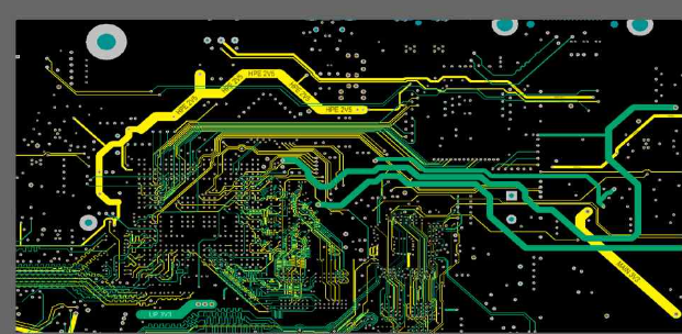
Printed Circuit Board (PCB) design involves numerous critical spacing considerations that directly impact the board’s functionality, reliability, and manufacturability. Clearance requirements in PCB design refer to the minimum distances that must be maintained between various components, traces, and other elements on the board. These requirements exist to prevent electrical interference, manufacturing defects, and potential safety hazards.
Understanding and properly implementing clearance requirements is essential for any PCB designer. This article will explore the various types of clearance requirements in PCB design, their importance, and how they affect the overall design process. We’ll examine electrical clearances, manufacturing clearances, thermal considerations, and other specialized spacing requirements that designers must account for in their layouts.
Electrical Clearance Requirements
High Voltage Clearances
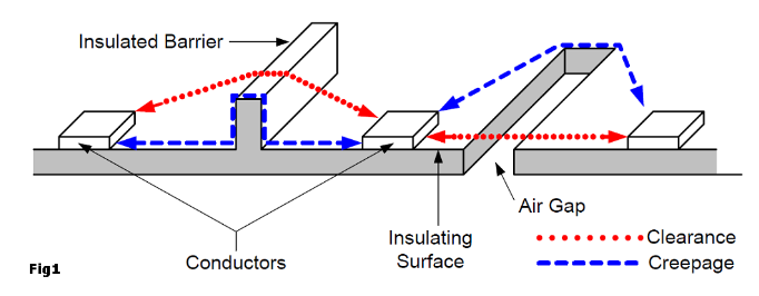
One of the most critical clearance requirements in PCB design involves high voltage applications. As voltage increases, the minimum distance between conductors must also increase to prevent arcing or breakdown through the air (creepage) or along the surface of the board (clearance).
For low-voltage designs (below 50V), typical clearance might be as small as 0.1mm, while high-voltage designs (above 1kV) may require several millimeters of spacing. The IPC-2221 standard provides guidelines for these clearances based on voltage levels and environmental conditions (indoor/outdoor, pollution degree).
Signal Integrity Clearances
Maintaining proper spacing between signal traces is crucial for preventing crosstalk and electromagnetic interference (EMI). Key considerations include:
- Trace-to-trace spacing: Typically 3-4 times the trace width for parallel runs
- High-speed signal isolation: Critical signals often require greater spacing or shielding
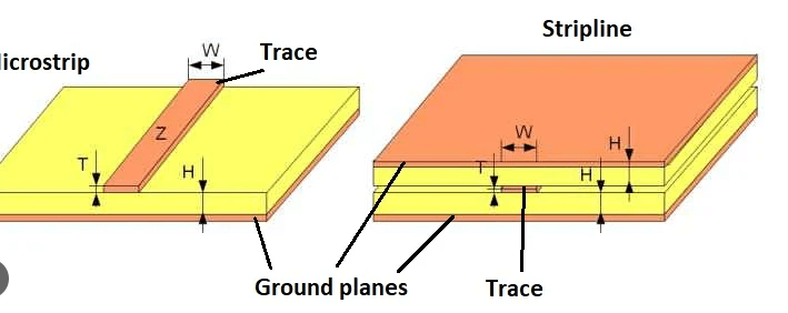
- Impedance control: Spacing affects impedance in controlled impedance designs
Power Plane Clearances
Power planes require special clearance considerations:
- Power-to-ground spacing in multilayer boards affects capacitance and noise
- Clearance around plane edges to prevent flashover
- Spacing between different voltage planes
Manufacturing Clearance Requirements
Fabrication Clearances
PCB manufacturers have specific capabilities and limitations that dictate minimum clearances:
- Minimum trace/space: The smallest possible gap between copper features (typically 3-6 mil for standard fabrication)
- Drill-to-copper: Spacing required between drilled holes and nearby copper (typically 8-10 mil)
- Board edge clearance: Copper features must be kept away from the board outline (typically 20 mil or more)
Solder Mask Clearances
Solder mask application requires careful spacing considerations:
- Solder mask web: Minimum bridge between solder mask openings (typically 3-5 mil)
- Solder mask expansion: How much the mask opening exceeds the pad size (typically 2-4 mil)
- Clearance between mask openings to prevent bridging
Silkscreen Clearances
Legibility and manufacturability dictate silkscreen spacing:
- Text-to-copper spacing to prevent overlap (typically 5-10 mil)
- Minimum line width for readable text (typically 5 mil)
- Clearance around components for assembly identification
Component Placement Clearances
Physical Component Spacing
Adequate space must be provided between components for:
- Assembly access (especially for manual soldering)
- Rework and repair
- Heat dissipation
- Mechanical clearance for connectors or moving parts
Land Pattern Clearances
Component footprints require specific spacing:
- Pad-to-pad spacing within a footprint
- Clearance between adjacent components’ pads
- Keepout areas for component bodies
Reflow and Wave Soldering Considerations
Different soldering processes impose unique clearance needs:
- Reflow: Components must not shadow others during heating
- Wave: Adequate spacing for solder wave contact
- Hand soldering: Space for tool access
Specialized Clearance Requirements
High-Frequency/RF Design Clearances
RF circuits have stringent spacing requirements:
- Controlled impedance trace spacing
- Isolation between RF sections
- Shielding requirements
High-Current Clearances
High-current traces need additional spacing:
- Prevent thermal effects on nearby components
- Account for potential conductor expansion
- Maintain adequate creepage for safety
Mixed-Signal Design Clearances
Combining analog and digital sections requires:
- Proper isolation between sensitive analog and noisy digital sections
- Careful ground plane partitioning
- Adequate spacing for noise reduction
Design Rule Checking (DRC) for Clearances
Implementing Clearance Rules in CAD Tools
Modern PCB design software allows designers to:
- Set up comprehensive clearance rules
- Define different spacing for various net classes
- Create area-specific rules
Common DRC Violations
Frequent clearance-related design rule check issues include:
- Insufficient pad-to-trace spacing
- Violations of high-voltage requirements
- Manufacturing clearance violations
Best Practices for Clearance Management
Effective strategies include:
- Creating a comprehensive clearance matrix
- Using hierarchical rule sets
- Implementing design templates for recurring projects
Industry Standards and Regulations
IPC Standards
Key IPC standards addressing clearance requirements:
- IPC-2221: Generic Standard on Printed Board Design
- IPC-7351: Land Pattern Design standards
- IPC-6012: Qualification and Performance Specification for Rigid PCBs
Safety Standards
Relevant safety standards include:
- UL 60950-1 (Information Technology Equipment)
- IEC 61010 (Measurement, Control, and Laboratory Equipment)
- IPC-9592 (Power Conversion Devices)
Industry-Specific Requirements
Certain industries have unique clearance needs:
- Automotive (high-vibration environments)
- Aerospace (extreme temperature variations)
- Medical (strict safety requirements)
Thermal Clearance Considerations
Heat Dissipation Spacing
Proper spacing helps manage thermal issues:
- Clearance around high-heat components
- Thermal relief in copper pours
- Airflow considerations
CTE Mismatch Accommodation
Accounting for coefficient of thermal expansion differences:
- Spacing for expansion in high-temperature applications
- Clearance around large components
- Board edge effects
Future Trends in PCB Clearance Requirements
Miniaturization Challenges
As PCBs shrink, clearance management becomes more critical:
- Advanced materials enabling smaller clearances
- High-density interconnect (HDI) technologies
- Embedded components
Advanced Manufacturing Capabilities
New fabrication methods affect clearance requirements:
- Fine-line etching capabilities
- Laser drilling for microvias
- Additive manufacturing approaches
Evolving Design Methodologies
Changing design practices influence clearance needs:
- 3D component modeling for accurate clearance checking
- AI-assisted design rule optimization
- Virtual prototyping for clearance validation
Conclusion
PCB design clearance requirements encompass a wide range of considerations that span electrical, manufacturing, thermal, and mechanical domains. Successful PCB designers must understand and carefully balance all these spacing requirements to create boards that are functional, reliable, and manufacturable. By implementing comprehensive design rules, staying current with industry standards, and leveraging modern design tools, engineers can effectively manage the complex clearance requirements in today’s PCB designs.
As technology continues to advance, clearance requirements will evolve, requiring designers to continually update their knowledge and adapt their design practices. The proper implementation of spacing requirements remains a fundamental aspect of quality PCB design that directly impacts product performance and reliability.