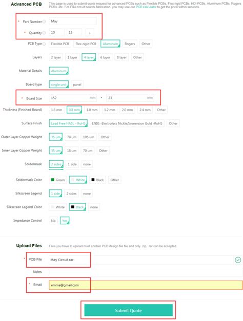
PCB Design Considerations for RGB Signal Impedance Control
Introduction
In modern electronic systems, RGB (Red, Green, Blue) signals play a critical role in video transmission and display technologies. Whether in consumer electronics like televisions and computer monitors or professional video equipment, maintaining signal integrity for RGB pathways is essential for high-quality image reproduction. One of the most crucial aspects of RGB signal PCB design is proper impedance control, which directly affects signal quality, electromagnetic compatibility (EMC), and overall system performance.
This article explores the key considerations for impedance control in RGB signal PCB design, covering fundamental concepts, calculation methods, routing techniques, and practical implementation strategies.
Understanding RGB Signal Characteristics
1. Signal Nature and Requirements
RGB signals typically carry analog video information with specific characteristics:
- Frequency content: Ranging from DC to several hundred MHz for high-resolution displays
- Voltage levels: Typically 0.7Vpp for standard video signals
- Signal matching: Precise timing and amplitude matching between R, G, and B channels is critical
2. Impedance Requirements
Most RGB video systems require controlled impedance transmission lines with:
- Characteristic impedance: Usually 75Ω for single-ended signals
- Tolerance: Typically ±10% or better
- Differential impedance: For differential RGB implementations (e.g., LVDS), usually 100Ω differential
Impedance Control Fundamentals
1. Transmission Line Theory Basics
At high frequencies, PCB traces behave as transmission lines where impedance is determined by:
Z₀ = √(L/C)Where:
- Z₀ = characteristic impedance
- L = inductance per unit length
- C = capacitance per unit length
2. Key Parameters Affecting Impedance
For surface microstrip traces (most common for RGB signals):
- Trace width (W)
- Dielectric thickness (H)
- Copper thickness (T)
- Dielectric constant (εᵣ)
- Solder mask presence and thickness
For stripline configurations:
- Same parameters as microstrip plus:
- Distance to second reference plane
Calculating RGB Signal Impedance
1. Microstrip Impedance Calculations
The simplified formula for microstrip impedance is:
Z₀ = [87/√(εᵣ+1.41)] × ln[5.98H/(0.8W+T)]Where:
- Z₀ in ohms
- H, W, T in mils (thousandths of an inch)
2. Stripline Impedance Calculations
For symmetric stripline:
Z₀ = [60/√εᵣ] × ln[4B/(0.67π(0.8W+T))]Where B is the total dielectric thickness between planes
3. Using PCB Stackup for Impedance Control
A typical 4-layer PCB stackup for RGB applications might be:
- Top Layer (RGB signals, components)
- Ground Plane
- Power Plane
- Bottom Layer (control signals)
Key parameters for a 75Ω microstrip on FR4 (εᵣ≈4.2):
- Dielectric thickness: 6-8 mils
- Trace width: 10-12 mils for 1oz copper
- Solder mask: Adds ~2-3Ω, must be accounted for
Practical PCB Design Guidelines
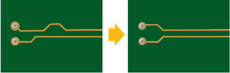
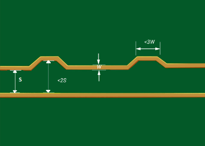
1. Routing Considerations
- Length matching: Keep R, G, B traces within ±50 mil length tolerance
- Separation: Maintain at least 3× trace width between RGB signals
- Corners: Use 45° angles or curved traces (avoid 90° turns)
- Vias: Minimize use (each via adds ~0.5-1pF discontinuity)
2. Reference Planes
- Provide unbroken ground reference beneath RGB traces
- Maintain at least 20 mil clearance from plane edges
- Avoid splits or gaps in reference planes under RGB paths
3. Termination Techniques
Proper termination is essential for impedance matching:
- Series termination: 22-33Ω resistors near driver
- Parallel termination: 75Ω to ground at receiver
- AC termination: RC networks for DC-coupled signals
4. Layer Transitions
When changing layers for RGB signals:
- Place ground vias adjacent to signal vias (<100 mil spacing)
- Keep transition regions as short as possible
- Consider using back-drilling for thick PCBs
Material Selection Considerations
1. Dielectric Materials
- Standard FR4: Cost-effective, εᵣ≈4.2-4.5 (frequency dependent)
- High-frequency laminates: Rogers, Isola materials with stable εᵣ
- Low-loss materials: For very long RGB paths (>12 inches)
2. Copper Weight
- 1oz (35μm): Standard, easier impedance control
- 0.5oz (18μm): Finer features, higher precision
- 2oz (70μm): For high-current applications (rare in RGB)
Verification and Testing
1. Simulation Tools
- 2D field solvers (Polar SI9000, Altium impedance calculator)
- 3D EM simulators (HFSS, CST) for complex structures
- Signal integrity analysis (HyperLynx, ADS)
2. Measurement Techniques
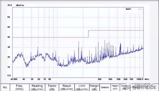
- Time Domain Reflectometry (TDR) for impedance verification
- Network analyzer for frequency domain characterization
- Eye diagram analysis for system-level validation
Common Design Pitfalls
1. Impedance Discontinuities
- Abrupt width changes
- Improper via transitions
- Connector interfaces
- Test point additions
2. Crosstalk Issues
- Insufficient spacing between RGB channels
- Parallel routing over long distances
- Shared reference current return paths
3. Grounding Problems
- Inadequate ground connections
- Ground loops in return paths
- Split plane crossings without proper bridging
Advanced Topics
1. Differential RGB Signaling
Some systems use differential pairs for RGB:
- LVDS, RSDS, or proprietary differential interfaces
- 100Ω differential impedance requirements
- Requires tight pair coupling and length matching
2. Embedded Components
- Thin-film resistors for termination
- Capacitive compensation for discontinuities
- Buried passive components
3. Flex PCB Considerations
- Different εᵣ for polyimide materials
- Thinner dielectrics require narrower traces
- Bending radius effects on impedance
Conclusion
Proper impedance control in RGB signal PCB design is essential for maintaining signal integrity and achieving high-quality video performance. By understanding the fundamental principles of transmission lines, carefully calculating impedance parameters, and implementing robust routing strategies, designers can create reliable RGB signal paths that meet stringent video quality requirements.
Key takeaways include:
- Maintain consistent 75Ω impedance (or specified value) throughout the RGB signal path
- Provide solid reference planes and proper termination
- Match lengths and routing characteristics between R, G, and B channels
- Verify designs through simulation and measurement
- Account for all materials and construction factors in impedance calculations
As display resolutions continue to increase and signal bandwidths expand, these impedance control techniques will become even more critical for successful RGB signal PCB design.