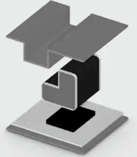
PCB design: DIP device assembly design defects
Understand DIP
DIP is a plug-in. The chip using this packaging method has two rows of pins, which can be directly soldered on a chip socket with a DIP structure or in a soldering position with the same number of solder holes. Its characteristics are that it can easily realize the perforation soldering of the PCB board and has good compatibility with the motherboard. However, due to its large packaging area and thickness, and the pins are easily damaged during the plug-in and unplug process, the reliability is poor.
DIP is the most popular plug-in package, and its application range includes standard logic IC, memory LSI, microcomputer circuit, etc., small outline package (SOP), derived SOJ (J-type pin small outline package), TSOP (thin small outline package), VSOP (very small outline package), SSOP (shrink SOP), TSSOP (thin shrink SOP) and SOT (small outline transistor), SOIC (small outline integrated circuit), etc.
DIP device assembly design defects
PCB package hole is larger than the device
PCB plug-in hole, package pin hole is drawn according to the specification book. In the plate making process, copper plating is required in the hole, and the general tolerance is plus or minus 0.075mm. If the PCB package hole is larger than the pin of the physical device, it will cause the device to loosen, insufficient tinning, empty soldering and other quality problems.
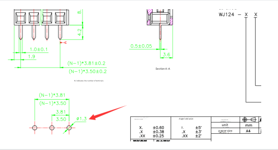
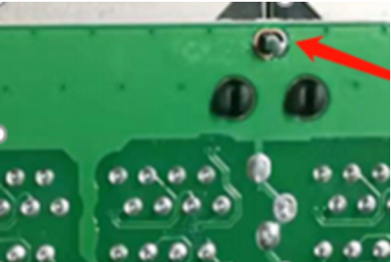
See the figure below. The device pin of WJ124-3.81-4P_WJ124-3.81-4P (KANGNEX) is 1.3mm, and the PCB package hole is 1.6mm. The large hole diameter leads to empty soldering during wave soldering.
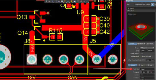
Continue with the above figure, purchase WJ124-3.81-4P_WJ124-3.81-4P (KANGNEX) components according to the design requirements. The pin 1.3mm is correct.
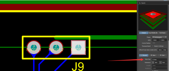
PCB package hole is smaller than the device
The hole on the solder pad of the plug-in component in the PCB board is small, and the component cannot be inserted. The only solution to this problem is to enlarge the hole diameter and then insert it, but there will be no copper in the hole. If it is a single or double-sided board, this method can be used. The outer layer of the single or double-sided board is electrically conductive, and it can be conductive after soldering. If the plug-in hole of the multi-layer board is small, the inner layer can only be redone if there is electrical conductivity. Because the inner layer is conductive, the hole cannot be enlarged to remedy it.
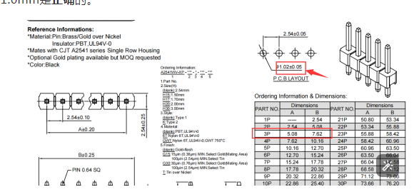
See the figure below. According to the design requirements, the components of A2541Hwv-3P_A2541HWV-3P (CJT) are purchased. The pin is 1.0mm, and the hole of the PCB package pad is 0.7mm, which makes it impossible to insert.
Continuing from the above figure, according to the design requirements, the components of A2541Hwv-3P_A2541HWV-3P (CJT) are purchased, and the pin 1.0mm is correct.
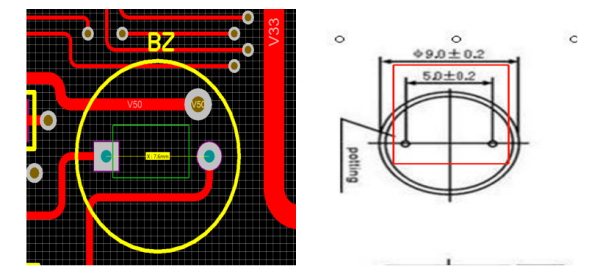
The package pin spacing is different from the device
The PCB package pad of the DIP device is not only consistent with the pin diameter, but also the pin spacing must be the same distance. If the pin hole spacing is inconsistent with the device, the device will not be inserted, except for components with adjustable pin spacing.
See the figure below, the PCB package pin hole spacing is 7.6mm, and the purchased component pin hole spacing is 5.0mm. The difference of 2.6mm makes the device unusable.
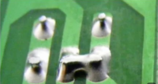
PCB package hole spacing is too close
When designing the package, pay attention to the distance between the pin holes. Even if the bare board can be generated with a small pin hole spacing, it is easy to cause a tin short circuit during wave soldering during assembly.
See the figure below. The tin short circuit may be caused by the small pin distance. There are many reasons for the tin short circuit during wave soldering. If the assemblability can be prevented in advance at the design end, the occurrence rate of the problem can be reduced.
DIP device pin problem case
The material size does not match the PCB pad hole size
Problem description
After a product DIP was wave soldered, it was found that the tin on the fixed foot pad of the network socket was seriously insufficient, which was a blank soldering.
Impact of the problem
The stability of the network socket and the PCB board deteriorates, and the signal pins are stressed during the use of the product, which eventually leads to the connection of the signal pins, affecting the product performance and causing the risk of failure during user use.
Problem extension
The stability of the network socket is poor, the connection performance of the signal pins is poor, and there are quality problems, which may bring safety hazards to users, and the final loss is unimaginable.
DIP device assembly analysis inspection
There are many problems related to DIP device pins, and many key points are easily overlooked, resulting in scrap boards in the end. So how to quickly and completely solve such problems at one time?
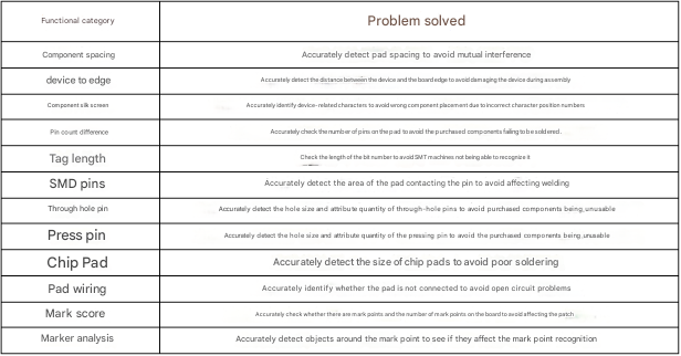
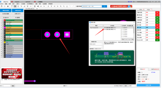
Here you can use the assembly analysis function of Huaqiu DFM software, which has a special inspection of the pins of DIP devices. The inspection items include the number of pins of through holes, THT pin limit, THT pin limit, and THT pin properties. The inspection items of the pins basically cover the problems that may occur in the design of DIP device pins.
After the PCB design is completed, the PCBA assembly analysis function can be used to discover design defects in advance, solve design anomalies before product production, and avoid design problems during the assembly process, delaying production time and wasting R&D costs.
Its assembly analysis function has 10 major items and 234 detailed inspection rules, covering all possible assembly problems, such as device analysis, pin analysis, pad analysis, etc., which can solve a variety of production situations that engineers cannot predict in advance.