PCB Design for Maintainability: Key Principles and Best Practices
Introduction
Printed Circuit Board (PCB) design is a critical aspect of electronic product development. While functionality, performance, and cost are often prioritized, maintainability is an equally important factor that impacts the long-term reliability and serviceability of electronic systems. A well-designed PCB should not only meet performance requirements but also facilitate easy troubleshooting, repair, and upgrades.
This article explores the key principles of PCB maintainability design, including layout considerations, component selection, testability, and documentation. By implementing these best practices, engineers can reduce downtime, lower repair costs, and extend the lifespan of electronic products.
1. Importance of Maintainability in PCB Design
Maintainability refers to the ease with which a PCB can be inspected, diagnosed, repaired, or modified. A maintainable PCB design offers several benefits:
- Reduced Downtime: Faster troubleshooting and repair minimize operational disruptions.
- Lower Repair Costs: Easily accessible components reduce labor and replacement expenses.
- Extended Product Lifespan: Upgradable and repairable designs prolong usability.
- Improved Serviceability: Well-documented and logically organized PCBs simplify maintenance.
To achieve these benefits, designers must consider maintainability early in the PCB development process.
2. Key Principles of Maintainable PCB Design
2.1. Logical and Modular Layout
A well-organized PCB layout enhances maintainability by grouping related components and functions. Key strategies include:
- Functional Partitioning: Divide the PCB into logical sections (e.g., power supply, signal processing, I/O interfaces) to isolate faults.
- Modular Design: Use subassemblies or plug-in modules for critical functions, allowing easy replacement.
- Standardized Interfaces: Ensure connectors and interfaces follow industry standards for compatibility.
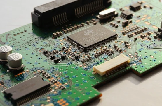
2.2. Component Selection and Placement
Choosing the right components and placing them strategically improves repairability:
- Avoid Obsolete Parts: Select components with long-term availability to prevent future sourcing issues.
- Use Standardized Footprints: Standardized packages (e.g., SOIC, QFP) simplify replacement.
- Minimize High-Risk Components: Place sensitive components (e.g., BGAs) in accessible locations.
- Provide Adequate Spacing: Ensure sufficient clearance for hand tools during rework.
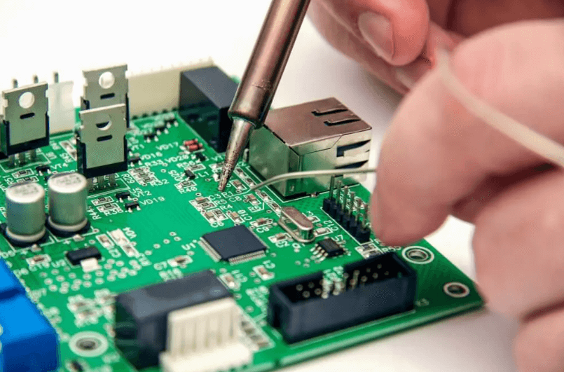
2.3. Accessibility for Testing and Rework
A maintainable PCB should allow easy access for testing and repairs:
- Test Points: Include exposed test points for critical signals (voltage, clock, data lines).
- Avoid Bottom-Side Components: If possible, place components on the top side for easier access.
- Use Through-Hole Components: They are easier to replace than surface-mount devices (SMDs).
- Avoid Underfill and Conformal Coating: Unless necessary, these can hinder rework.
2.4. Clear Labeling and Documentation
Proper documentation ensures efficient maintenance:
- Component Designators: Clearly label all components (e.g., R1, C2, U3) for easy identification.
- Polarity Markings: Indicate polarity for diodes, capacitors, and connectors.
- Revision Control: Maintain versioned schematics and layout files.
- Service Manuals: Provide troubleshooting guides and expected signal values.
2.5. Design for Testability (DFT)
Incorporating testability features simplifies diagnostics:
- Boundary Scan (JTAG): Supports automated testing for complex PCBs.
- Built-in Self-Test (BIST): Integrate self-diagnostic circuits for critical functions.
- Flying Probe Access: Ensure test pads are accessible for automated testing.
2.6. Thermal and Mechanical Considerations
Overheating and mechanical stress can lead to failures. Maintainable designs should:
- Use Robust Connectors: Select high-durability connectors for frequent mating cycles.
- Implement Thermal Relief: Prevent solder joint cracks due to thermal cycling.
- Secure Heavy Components: Use additional mechanical support for large parts (e.g., transformers).
3. Common Maintainability Pitfalls and How to Avoid Them
3.1. Overcrowded Layouts
Problem: Dense component placement makes rework difficult.
Solution: Follow IPC spacing guidelines and prioritize serviceability.
3.2. Lack of Test Points
Problem: No access to critical signals for debugging.
Solution: Add test points for power, ground, and key signals.
3.3. Poor Documentation
Problem: Missing or outdated schematics delay repairs.
Solution: Maintain up-to-date design files and assembly notes.
3.4. Non-Standard Components
Problem: Custom or obsolete parts complicate replacements.
Solution: Use industry-standard components whenever possible.

4. Case Study: Maintainability in Industrial PCBs
An industrial control system PCB was redesigned for better maintainability by:
- Implementing modular power supply sections.
- Adding test points for all critical signals.
- Using socketed microcontrollers for easy upgrades.
- Providing detailed service documentation.
Result: Repair time decreased by 40%, and field service costs dropped significantly.
5. Conclusion
Designing PCBs for maintainability is essential for reducing lifecycle costs and improving product reliability. By following best practices in layout, component selection, testability, and documentation, engineers can create PCBs that are easier to service, repair, and upgrade.
Investing in maintainability early in the design phase pays off in the long run, ensuring that electronic products remain operational and cost-effective throughout their lifespan.


