pcb Design for Manufacturing Analysis (DFM System)
“DFM” – a three-letter abbreviation, its meaning varies from insignificant to crucial depending on the role you play in the design and manufacturing process chain.
In today’s electronics industry, there are several forces driving the process of Design for Manufacturing (DFM), the three most common of which are:
Increased component density brought about by new technologies
The need to shorten design cycle time
The implementation of outsourcing and overseas manufacturing models
The increasing demand for smaller and lighter designs with more functions has brought us new printed circuit board manufacturing technologies, such as sequential stacking, embedded passive and active component design, and component packaging technology innovations such as Micro-BGA, CSP and POP. All of this makes PCB design, production and assembly more complicated.
Reducing “time to market” is a pressing need.
Since the iteration of PCB design may increase the design cycle by several weeks on average, thus delaying the time to market of the product, it is absolutely necessary to eliminate manufacturability problems (one of the important reasons for design iteration) as early as possible in PCB design time.
It is generally believed that DFM is simply performing some basic error checks on the PCBCAD system to ensure that the lines will not short when the PCB is manufactured, or to ensure that the parts will not interfere with each other when the PCB is assembled.
In fact, DFM results mean that the design has been optimized to the greatest extent possible, ensuring that the product can be manufactured, assembled and tested in the most efficient way – eliminating unnecessary processes that may cause additional time and cost. A fully optimized design even takes into account the manufacturing yield of the product.
Now let’s take a step back and see what users want to achieve with the design for manufacturability (DFM) process when designing PCBs.
It is generally accepted that the design of a product has a significant and measurable impact on the manufacturing cycle and unit product cost. In other words, a bad design will lead to longer manufacturing time and higher costs. With the ever-present pressure to reduce costs and shorten product time to market, the ultimate goal of implementing DFM is to achieve cost-effective manufacturing. This will be achieved by maintaining high yield (low scrap) and minimizing design revisions. At the same time, we also need to realize that the application of DFM enables the full utilization of process capabilities, such as the application of new technologies to concentrate the design from two PCBs to one PCB, thus saving both time and cost.
The use of DFM is not just to answer the question “Can this design be manufactured?”, but to answer the question “Can this design be manufactured efficiently and profitably?”
Most importantly, DFM must be viewed as an operational logic throughout the entire New Product Introduction (NPI) process chain. It is not an afterthought or an additional supplement after the design is completed. Yes, there are stand-alone applications that can be identified as DFM tools, but in general, design for manufacturability (DFM) tools must be embedded in all tools and ensured by the pre-definition of necessary rules and the implementation of these rules throughout the tool chain. Many PCB design tools conform to this model through a rule-based design philosophy, and the design tools either directly follow the rules or at least can do rule checking.
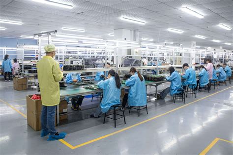
Manufacturing (or production) needs to be divided into several major parts, each with significant and independent content, namely PCB fabrication, assembly and test.
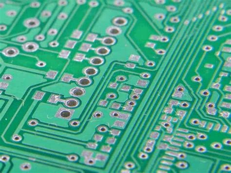
PCB fabrication includes all steps related to bare board production of printed circuit boards (including testing and verification to ensure good quality).
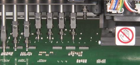
Assembly is the process of placing the required parts on the bare board, and it may also include system assembly (e.g. assembling the PCB into a system to form a complete product).
Testing includes ICT testing (ensuring correct part placement, including correct part orientation, part values and correct operation) and functional testing (verifying the operational function of the entire board – does it achieve all the designed functions?). Testing content also includes visual inspection and repair/rework issues.
Each of the above parts has its own special needs, and each aspect must be considered to ensure good DFM results. It is obviously not enough to use DFM to check whether the PCB can be manufactured, but then it cannot be automatically assembled – especially when you need to produce thousands of boards.
If you only ensure that the design does not go wrong during manufacturing, you miss a major factor that has a significant impact on time and cost during manufacturing.
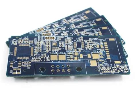
In addition to checking the design data content according to specifications or rules (object size, spacing, spacing, etc.), you also need to look at the type and number of processes required to manufacture the design. For example, if the designer uses only a plug-in component in the design, he immediately and automatically introduces one or more additional processes in the manufacturing chain (such as automatic insertion and wave soldering) – this will obviously have a significant impact on the cost of each board, which can be avoided by using equivalent SMD components instead. Similarly, choosing a “special-shaped” part that cannot be automatically inserted in the design may require an additional manual assembly station, which can be avoided by careful selection of parts. In the PCB manufacturing part, the design from double-sided boards to multi-layer boards, from through-holes to blind vias, will lead to additional processes and more potential factors for errors, which can be avoided through DFM analysis.
There are two levels of DFM analysis.
The first includes simpler or “general” tests (such as those applicable to all manufacturers and are not affected by the manufacturer’s process capabilities). This category includes simple part shape size and spacing checks, using 2D placement shapes to check part layouts, etc. While these factors can prevent manufacturing errors to some extent (assuming that appropriate rules have been set in advance), they tend to provide “worst case” results and do not give designers enough help in how to better utilize existing technologies and process capabilities.
The second level of DFM analysis requires detailed and accurate modeling of the process used, such as consideration of the actual part shape and the capabilities of the placement equipment (types of parts that can be handled, geometry of the pick-up head/gripper, insertion sequence).
However, to obtain good second-level analysis results, process simulation needs to be performed based on the production capabilities of a specific manufacturer.
PCB board production inspection needs to be performed based on the process capabilities of the selected manufacturer; assembly inspection requires knowing what assembly equipment is available and its settings. A clearer understanding of the equipment capabilities for testing, inspection, and rework must also be obtained. All of this is not easy to do, especially for companies that do not manufacture in-house, because it is not easy to obtain such detailed process information from external contract manufacturers (CEMs).
In addition, only referring to the design data content does not give a comprehensive consideration.
The setup of assembly equipment (assigning parts to bins), the order of assembling equipment on the line, balancing the line to achieve optimal output, etc. are all factors that need to be considered and software must be used. Although some may think of these as part of production planning, they are essential to a good DFM process and demonstrate the importance of tasks such as part selection and how detailed knowledge of the assembly process setup can help designers move towards designing products that can be manufactured efficiently.
Due to the number and complexity of rules, it is impossible for PCBCAD tools to handle all of them, either automatically or interactively; especially if we consider checks for thermal, signal integrity, electromagnetic effects, etc.
Therefore, specialized analysis tools must be used in conjunction to identify potential problems, provide suggestions on how to solve the problems, and allow users to adjust and trade off the relative impact of each rule violation.
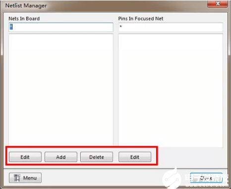
These specialized tools provide more than just the “go/no-go” checks that PCBCAD tools usually provide (see figure)
They can be configured to provide a severity level for the problem, giving the designer or NPI engineer more accurate information. This allows you to make more informed decisions about which issues must be addressed (e.g., not manufacturable), which issues are best addressed (can be manufactured with special permission), which issues can be safely ignored (no impact on manufacturing/yield), etc. With the built-in calculator, a variety of replacements can be made to try out rule legality.
In summary: PCB design for manufacturability analysis (DFM system) is a powerful tool to promote productivity. It can enable you to make your design more miniaturized without loss, reduce product time to market and confidently benefit from global manufacturing trends. If you don’t use DFM, you may face a huge challenge with high cost and high risk.