PCB Design Skills for RF Circuits
Today, PCB technology mainly changes according to the characteristics and requirements of electronic products. In recent years, electronic products have become more and more multifunctional, sophisticated and compliant with environmental regulations. Therefore, the precision of PCB is increasing, and its soft and hard board combination application will also increase.
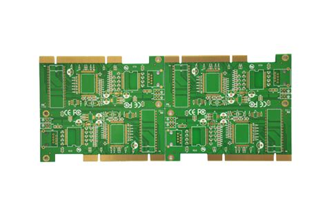
PCB is the foundation of the information industry.
From computers to portable electronic devices, almost all electronic and electrical products have circuit boards. With the development of communication technology, handheld wireless RF circuit technology is becoming more and more widely used. One of the biggest features of these devices (such as mobile phones, wireless PDAs, etc.) is: first, it almost covers all portable subsystems; second, miniaturization, and miniaturization means that the density of components is very high, which makes the mutual interference of components (including SMD, SMC, bare chips, etc.) very prominent. Therefore, it has become a very important topic to design a perfect PCB for RF circuits and audio circuits to prevent and suppress electromagnetic interference and thus improve electromagnetic compatibility.
Because the same circuit, different PCB design structures, its performance indicators will vary greatly. Especially as the audio functions of today’s handheld products continue to increase, more attention must be paid to the PCB layout of audio circuits. Based on this, this article analyzes and explains the ingenious design of PCBs for RF circuits and audio circuits of handheld products (including component layout, component placement, wiring and grounding techniques).
1.Component layout
First, the general layout principle: components should be arranged in the same direction as much as possible, and the phenomenon of poor soldering can be reduced or even avoided by selecting the direction in which the PCB enters the tin melting system; from practice, it is known that there must be at least 0.5mm spacing between components to meet the tin melting requirements of components. If the space of the PCB board allows, the spacing between components should be as wide as possible. For double-sided boards, one side should generally be designed for SMD and SMC components, and the other side for discrete components.
1.1 Divide the PCB into digital and analog areas
The first step in any PCB design is of course to select the PCB placement of each component. We call this step “board layout consideration”. Careful component layout can reduce signal interconnection, ground line segmentation, noise coupling and the area occupied by the circuit board.
Electromagnetic compatibility requires that each circuit module PCB design should not generate electromagnetic radiation as much as possible and have a certain anti-electromagnetic interference ability. Therefore, the layout of components also directly affects the interference and anti-interference ability of the circuit itself, which is also directly related to the performance of the designed circuit.
Therefore, in addition to considering the layout of ordinary PCB design when designing RF circuit PCB, it is also necessary to consider how to reduce the mutual interference between the various parts of the RF circuit, how to reduce the interference of the circuit itself to other circuits, and the anti-interference ability of the circuit itself.
From experience, the effect of RF circuit depends not only on the performance indicators of the RF circuit board itself, but also on the mutual influence with the CPU processing board. Since RF circuit contains digital circuit and analog circuit, in order to prevent digital noise from interfering with sensitive analog circuit, the two must be separated. Dividing PCB into digital area and analog area helps to improve the layout of such circuits, which is particularly important.
1.2 Need to prevent RF noise from coupling to audio circuit
Although the RF part of handheld products is usually treated as an analog circuit, a common problem that needs to be paid attention to in many designs is RF noise. It is necessary to prevent RF noise from coupling to audio circuit because RF noise generates audible noise after demodulation. In order to solve this problem, the RF circuit and the audio circuit need to be separated as much as possible. After dividing the PCB into analog and digital, the component layout of the analog part needs to be considered. The component layout should make the path of the audio signal as short as possible. The audio amplifier should be placed as close to the headphone jack and speaker as possible to minimize the EMI radiation of the Class D audio amplifier and the coupling noise of the headphone signal. The analog audio signal source must be as close to the input of the audio amplifier as possible to minimize the input coupling noise. All input leads are an antenna for RF signals. Shortening the lead length helps reduce the antenna radiation effect in the corresponding frequency band.
2.Issues to be noted in component layout and application examples
2.1 Issues to be noted in layout:
Carefully analyze the circuit structure. Process the circuit in blocks (such as high-frequency amplifier circuit, mixer circuit and demodulation circuit, etc.), separate strong electric signals from weak electric signals as much as possible. After separating the digital signal circuit and the analog signal circuit, it should also be noted that the circuits that complete the same function should be arranged within a certain range as much as possible to reduce the signal loop area; the filter network of each part of the circuit must be connected nearby, which can not only reduce radiation, but also reduce the probability of interference and improve the anti-interference ability of the circuit.
Group the unit circuits according to their different sensitivity to electromagnetic compatibility during use. When laying out the components of the circuit that are susceptible to interference, the interference source should be avoided as much as possible (such as interference from the CPU on the data processing board, etc.).
2.2 Examples of the impact of component layout on audio signals
The impact of unreasonable component layout on audio signal quality
There are two more serious problems with an unreasonable audio component layout: one is that the audio amplifier is too far away from the audio signal source, and the lead wire passes through the noisy digital circuit and switch circuit, which increases the probability of noise coupling. Longer leads also enhance the RF antenna effect. If the mobile phone uses GSM technology, these antennas can pick up the GSM transmission signal and feed it into the audio amplifier. Almost all amplifiers can demodulate the 217Hz envelope to some extent, generating noise at the output. In the worst case, the noise may completely drown out the audio signal. Shortening the length of the input lead can effectively reduce the noise coupled to the audio amplifier. The second audio is that the amplifier is too far away from the speaker and headphone jack. If the audio amplifier uses a Class D amplifier, the longer headphone lead will increase the EMI radiation of the amplifier. This radiation may cause the device to fail the test standards set by the local government. Longer headphone and microphone leads will also increase the lead impedance and reduce the power that the load can obtain. Finally, because the components are arranged so dispersed, the connection between components will have to pass through other subsystems. This will increase the wiring difficulty not only of the audio part, but also of other subsystems.
Schematic diagram of the impact of unreasonable component layout on audio signal quality
Reasonable component layout improves audio signal quality
The arrangement of the same components, rearranged components can make more efficient use of space and shorten the lead length. Note that all audio circuits are distributed near the headphone jack and speaker, the audio input and output leads are much shorter than the above solution, and no audio circuits are placed in other areas of the PCB. Such a design can comprehensively reduce system noise, reduce RF interference, and simplify wiring.
A reasonable component layout shows the improvement of audio signal quality
3.Wiring principles and techniques
After the layout of components is basically completed, wiring can be started.
3.1 Basic principles of wiring
When the assembly density permits, try to use low-density wiring design, and the signal routing should be as consistent as possible, which is conducive to impedance matching.
For RF circuits, unreasonable design of the direction, width, and line spacing of signal lines may cause cross interference between signal transmission lines. The signal path has very limited impact on audio output noise and distortion, that is, the compromise measures required to ensure performance are very limited. Audio amplifiers are usually powered directly by batteries and require considerable current. If long and thin power leads are used, the power ripple will increase. Compared with short and wide leads, long and thin leads have larger impedance, and the current changes generated by the lead impedance will be converted into voltage changes and fed into the device. To optimize performance, the amplifier power supply should use the shortest possible leads. Differential signals should be used whenever possible. Differential inputs have higher noise suppression, allowing differential receivers to suppress common-mode noise on positive and negative signal lines. To fully utilize the advantages of differential amplifiers, it is very important to keep the same length of differential signal line pairs during routing, so that they have the same impedance and are as close to each other as possible to make their coupled noise the same. The differential input of the amplifier is very effective in suppressing noise from the system digital circuit. In addition, the system power supply itself also has noise interference, so when designing the RF circuit PCB, it is necessary to comprehensively consider and reasonably route.
3.2 Routing skills
When routing, all traces should be kept away from the border of the PCB board (about 2mm) to avoid disconnection or the risk of disconnection during PCB board production. The power line should be as wide as possible to reduce loop resistance. At the same time, the direction of the power line and ground line should be consistent with the direction of data transmission to improve anti-interference ability; the signal line should be as short as possible and the number of vias should be minimized; the connection between components should be as short as possible to reduce distributed parameters and mutual electromagnetic interference; incompatible signal lines should be kept away from each other and parallel routing should be avoided as much as possible, and the signal lines on the two positive sides should be perpendicular to each other; when wiring, the address where the corner is required should be 135°, and right angles should be avoided.
4.Grounding
In the PCB design of radio frequency circuits, the correct wiring of power lines and ground lines is particularly important, and reasonable design is the most important means to overcome electromagnetic interference. Quite a lot of interference sources on PCB are generated by power and ground lines, among which the noise interference caused by ground lines is the largest. The main reason why ground lines are prone to electromagnetic interference is that there is impedance in the ground line. When current flows through the ground line, voltage will be generated on the ground line, thereby generating ground line loop current and forming ground line loop interference. When multiple circuits share a ground line, common impedance coupling will be formed, thus generating the so-called ground line noise. Therefore, when routing the ground line of the RF circuit PCB, the following should be done:
Divide the circuit into blocks. The RF circuit can basically be divided into high-frequency amplification, mixing, demodulation, local oscillation and other parts. Provide a common potential reference point for each circuit module PCB design, that is, the ground line of each module circuit, so that the signal can be transmitted between different circuit modules PCB design. Then, it is summarized at the place where the RF circuit PCB is connected to the ground line, that is, the total ground line. Since there is only one reference point, there is no common impedance coupling, and thus there is no mutual interference problem.
The digital area and the analog area should be isolated by ground lines as much as possible, and the digital ground and the analog ground should be separated, and finally connected to the power ground.
When space permits, it is best to isolate the modules with ground lines to prevent signal coupling effects between each other.
For audio circuits, grounding is crucial to whether the performance requirements of the audio system can be met. There are two important considerations for grounding in any system: first, it is the return path for current flowing through the device, and second, it is the reference potential of digital and analog circuits. Here are some tips that apply to all systems:
Establish a continuous ground plane for digital circuits. The digital current in the ground layer returns through the signal path. The area of the loop should be kept to a minimum to reduce the antenna effect and parasitic inductance. Ensure that all digital signal leads have corresponding ground paths. This layer should cover the same area as the digital signal leads and have as few breaks as possible. Breaks in the ground layer, including vias, will cause the ground current to flow through a larger loop, thus generating greater radiation and noise.
Ensure ground current isolation. The ground currents of digital and analog circuits should be kept isolated to prevent digital currents from interfering with analog circuits. To achieve this goal, components need to be arranged correctly. If the analog circuit is arranged in one area of the PCB and the digital circuit is arranged in another area, the ground current will be naturally isolated. It is best to have an independent PCB layer for the analog circuit.
The analog circuit uses star grounding. Star grounding is to regard one point of the PCB as a common ground point, and only this point is regarded as the ground potential. In cellular phones, the battery ground terminal is usually used as the star ground point. The current flowing into the ground plane will not automatically disappear. All ground currents will be merged into this ground point. Audio amplifiers draw considerable current, which can affect the reference ground of the circuit itself and other systems. To address this problem, it is best to provide a dedicated return loop to bridge the amplifier’s power ground and the ground return of the headphone jack. Note that these dedicated loops should not cross digital signal lines because they will block digital return currents.
Maximize the role of bypass capacitors. Almost all devices require a bypass capacitor to provide transient currents that the power supply cannot provide. These capacitors should be placed as close to the power pins as possible to reduce parasitic inductance between the capacitor and the device pins, which will reduce the role of the bypass capacitor.
5.Conclusion
Designing a good PCB is a time-consuming and challenging task, but this investment is indeed worth it. Good PCB layout helps reduce system noise, improve RF signal suppression, and reduce signal distortion. Good PCB design also improves EMI performance and may require less shielding. If the PCB is not reasonable, problems that could have been avoided will occur during the testing phase. If measures are taken at this time, it may be too late and it will be difficult to solve the problems faced. It requires more time and effort, and sometimes additional components, increasing system cost and complexity.


