PCB Desmearing and Hole Wall Control: Techniques and Best Practices
Abstract
This paper examines the critical processes of desmearing and hole wall conditioning in printed circuit board (PCB) manufacturing. As modern PCBs continue to evolve with higher density interconnects and smaller via diameters, proper removal of drilling debris and smear material becomes increasingly essential for reliable plating and electrical performance. The article details current chemical and mechanical desmearing technologies, process control parameters, and quality verification methods. Special emphasis is placed on the relationship between desmearing effectiveness and subsequent metallization quality, including coverage, adhesion, and reliability.
1. Introduction
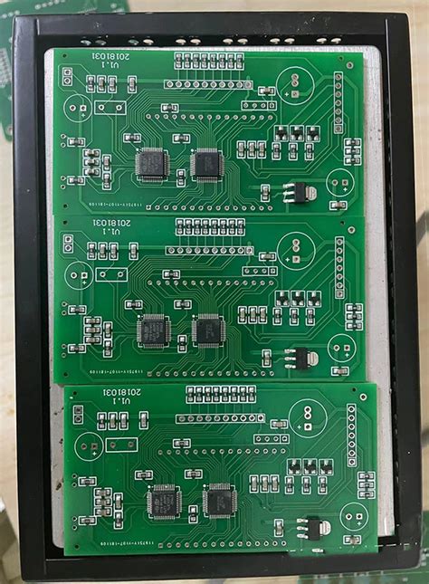
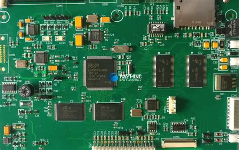
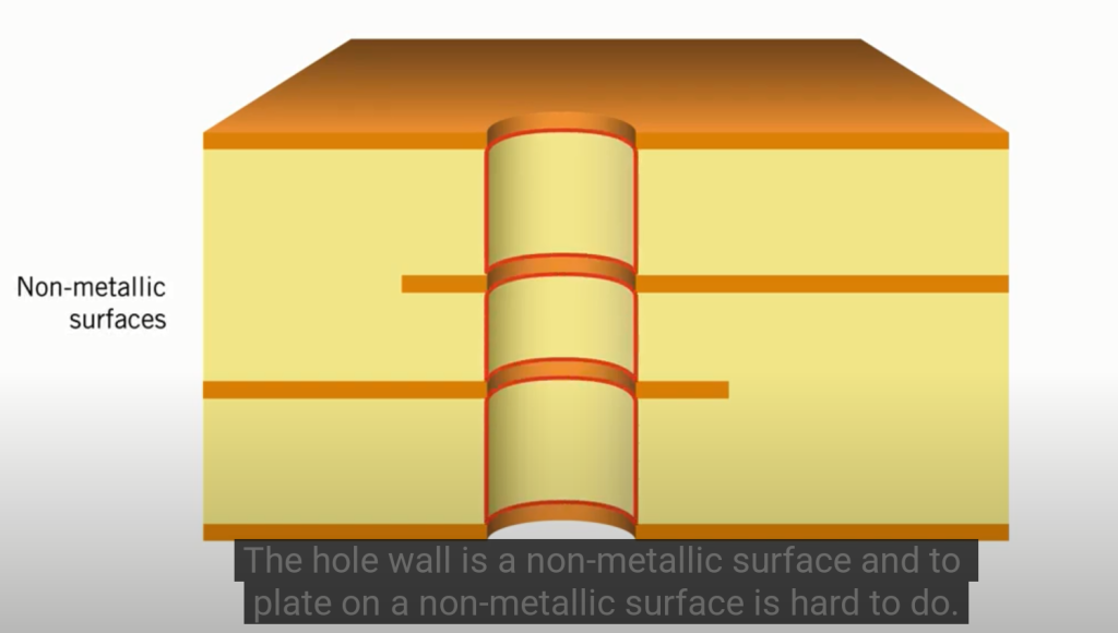
Printed circuit board manufacturing involves numerous precision processes where hole wall preparation plays a pivotal role in final product quality. During mechanical drilling of multilayer boards, the tremendous heat generated (180-220°C) melts the resin component of the substrate, creating a smear layer that coats the hole walls and covers exposed copper layers in buried and blind vias. This non-conductive epoxy smear must be completely removed to establish proper electrical connections between layers during subsequent plating processes.
Similarly, the mechanical drilling process leaves behind microscopic roughness and fractures in the hole walls that require conditioning to ensure uniform plating thickness and prevent voids or cracks that could lead to interconnect failures. The dual processes of desmearing (removing resin smear) and hole wall conditioning (improving surface characteristics) together determine the metallurgical quality of plated through holes (PTH) and microvias.
2. Desmearing Process Technologies
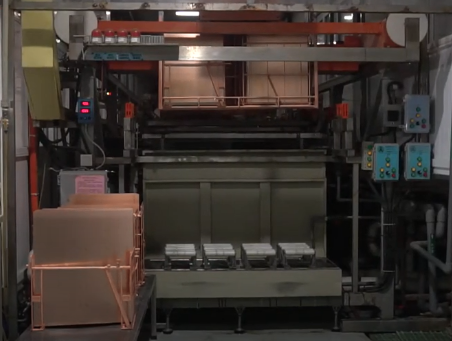
2.1 Chemical Desmearing Methods
Permanganate Systems: The most widely used chemical desmearing method employs alkaline permanganate solutions (typically potassium permanganate) which oxidize and degrade the resin smear. Modern permanganate systems operate in three stages:
- Swelling (typically using glycol ether solvents at 70-80°C)
- Oxidative attack (KMnO₄ solution at 80-90°C)
- Neutralization/reduction (acidic solutions with hydroxylamine or other reducing agents)
The permanganate concentration (60-100 g/L), temperature, and immersion time must be carefully controlled based on the resin system being processed. High Tg materials and polyimide substrates often require more aggressive parameters.
Sulfuric Acid Systems: Concentrated sulfuric acid (90-98%) at elevated temperatures (40-60°C) can effectively dissolve resin smear, particularly for PTFE and other exotic substrates. This method requires careful rinsing and neutralization steps.
Plasma Desmearing: Vacuum plasma systems using oxygen/CF₄ or oxygen/argon gas mixtures provide anisotropic etching of resin smear, especially valuable for high aspect ratio (8:1 or greater) microvias. Plasma systems eliminate chemical waste but have higher capital costs and slower throughput.
2.2 Mechanical Desmearing Methods
Pumice Scrubbing: Abrasive slurries containing pumice or aluminum oxide particles are sprayed at high pressure (2-4 bar) to mechanically scour hole walls. This method is less effective for multilayer boards with buried copper layers.
Brush Deburring: Rotating nylon brushes with abrasive particles can remove entry/exit burrs and mild smear but cannot reach mid-hole regions effectively.
Ultrasonic Cleaning: High frequency (25-40 kHz) ultrasonic tanks help remove loosened debris after chemical treatment but are not a primary desmearing method.
3. Hole Wall Conditioning
After desmearing, the hole walls require surface modification to optimize adhesion and plating uniformity:
3.1 Etchback Processes
Controlled micro-etching of the dielectric (usually 1-5 μm) creates anchor points for mechanical interlocking of the plated copper. For FR-4 materials, this is typically accomplished with:
- Sulfuric acid/hydrogen peroxide mixtures
- Ammoniacal etchants for high Tg materials
- Special formulations for Rogers and other low-loss substrates
3.2 Surface Roughening
Mechanical abrasion or chemical micro-etching increases surface area and creates the ideal profile for metallization:
- Optimal Rz (mean roughness depth): 1-3 μm
- Excessive roughness (>5 μm) can cause plating voids
- Insufficient roughness (<0.5 μm) risks poor adhesion
3.3 Catalyzation and Activation
For direct metallization processes (as opposed to traditional electroless copper), the conditioned surface requires proper catalytic treatment:
- Palladium/tin colloidal systems
- Ionic palladium activation
- Carbon or conductive polymer deposition
4. Process Control Parameters
Effective desmearing and hole wall control requires monitoring of multiple parameters:
| Parameter | Typical Range | Measurement Method |
|---|---|---|
| Permanganate concentration | 60-100 g/L | Titration (oxalate method) |
| Sweller temperature | 70±5°C | Digital thermometer |
| Oxidizer temperature | 85±3°C | PT100 sensor |
| Etchback depth | 1-5 μm | Cross-section microscopy |
| Rinsing water quality | <50 μS/cm | Conductivity meter |
| Solution turnover | 3-5 m²/ℓ | Process tracking |
Critical control factors include:
- Solution agitation (air or mechanical)
- Racking density (typically 0.5-1.5 dm²/ℓ)
- Process time (swelling: 3-7 min; oxidizer: 5-12 min)
- Filtration systems (25-50 μm filters)
5. Quality Verification Methods
5.1 Destructive Testing
- Microsectioning: Measures etchback depth, plating uniformity, and checks for residual smear
- Thermal Stress Testing: 288°C solder float for 10-20 seconds reveals plating weaknesses
- Peel Strength Testing: Measures copper adhesion (typically >1.0 N/mm)
5.2 Non-Destructive Testing
- Automated Optical Inspection (AOI): Checks for visible defects at 10-50× magnification
- Electrical Testing: Continuity testing of daisy chain structures
- Impedance Testing: For high frequency boards, verifies hole wall consistency
5.3 Process Control Samples
- Coupon Monitoring: Regular testing of designated test coupons on production panels
- SEM Analysis: Scanning electron microscopy for detailed surface examination
- EDS Analysis: Energy dispersive X-ray spectroscopy detects chemical residues
6. Advanced Materials Considerations
Modern PCB materials present unique desmearing challenges:
High Tg Materials: (Tg >170°C)
- Require higher permanganate concentrations (up to 120 g/L)
- Extended process times (up to 15 minutes oxidizer exposure)
- May need multiple processing cycles
Low-loss Materials: (e.g., PTFE, ceramic-filled)
- Often require plasma desmearing
- Special swelling agents (fluorocarbon solvents)
- Careful rinse control to prevent reprecipitation
Hybrid Constructions: (mixed dielectric materials)
- May need sequential processing
- Risk of over-etching softer materials
- Requires customized process development
7. Environmental and Safety Considerations
Modern desmearing processes must address:
- Wastewater Treatment: Permanganate reduction, neutralization
- Air Emissions: Volatile organic compounds from swellers
- Operator Safety: Thermal burns, chemical exposure
- Resource Recovery: Copper recovery from etchants, manganese recycling
Best practices include:
- Closed-loop recycling systems
- Automated chemical analysis and dosing
- Ergonomic equipment design
- Waste minimization protocols
8. Future Trends
Emerging technologies in hole preparation include:
- Supercritical CO₂ Cleaning: For residue-free surfaces
- Nanoparticle Catalyzation: For finer feature metallization
- Laser Desmearing: Precision treatment of microvias
- Biodegradable Chemicals: Reducing environmental impact
- Inline Process Monitoring: Real-time analytics for Industry 4.0
9. Conclusion
Proper desmearing and hole wall conditioning remain fundamental to PCB reliability, especially as designs push the limits of density and performance. Manufacturers must carefully select and control these processes based on their specific materials and product requirements. Continuous monitoring and adaptation to new substrate technologies will be essential as the industry progresses toward ever more demanding applications in 5G, automotive, and aerospace electronics.
By implementing robust desmearing and hole wall control processes with appropriate verification methods, PCB manufacturers can significantly improve yields and field reliability while meeting increasingly stringent performance requirements. The future will bring both challenges and opportunities as new materials and miniaturization trends demand innovative approaches to these fundamental processes.