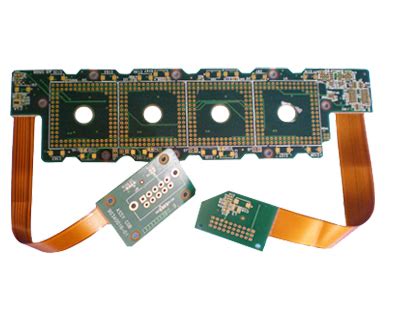
PCB EMI Shielding: Techniques and Best Practices
Introduction
Electromagnetic interference (EMI) is a significant concern in the design and manufacturing of printed circuit boards (PCBs). EMI can disrupt the performance of electronic devices, leading to malfunctions, data corruption, and even complete system failures. As electronic devices become more complex and operate at higher frequencies, the need for effective EMI shielding becomes increasingly critical. This article explores the various techniques and best practices for PCB EMI shielding, providing a comprehensive guide for engineers and designers.
Understanding EMI
What is EMI?
EMI refers to the disturbance generated by an external source that affects an electrical circuit by electromagnetic induction, electrostatic coupling, or conduction. This disturbance can degrade the performance of the circuit or even cause it to fail. EMI can be categorized into two types:
- Radiated EMI: This type of EMI is transmitted through the air and can affect nearby electronic devices. It is often caused by high-frequency signals, such as those generated by clock signals, switching power supplies, and RF circuits.
- Conducted EMI: This type of EMI is transmitted through conductive paths, such as power lines or signal cables. It can be caused by power supply noise, ground loops, or improper grounding.
Sources of EMI
EMI can originate from both internal and external sources:
- Internal Sources: These include components on the PCB itself, such as clock generators, switching regulators, and high-speed digital circuits. These components can generate electromagnetic fields that interfere with other parts of the circuit.
- External Sources: These include other electronic devices, power lines, and even natural phenomena like lightning. External EMI can be particularly challenging to mitigate, as it is often beyond the control of the PCB designer.
Importance of EMI Shielding in PCB Design
EMI shielding is essential for ensuring the reliable operation of electronic devices. Without proper shielding, EMI can cause a range of issues, including:
- Signal Integrity Problems: EMI can distort signals, leading to data errors and reduced performance.
- Increased Noise Levels: EMI can increase the noise floor, making it difficult to detect weak signals.
- Regulatory Compliance: Many electronic devices must comply with EMI regulations, such as those set by the Federal Communications Commission (FCC) in the United States or the European Union’s EMC Directive. Failure to comply can result in costly redesigns and delays in product launches.
Techniques for PCB EMI Shielding
There are several techniques for mitigating EMI in PCB design. These techniques can be broadly categorized into two approaches: prevention and containment.
Prevention Techniques
Prevention techniques aim to minimize the generation of EMI at the source. These techniques include:
1. Proper Component Placement
- Separation of High-Speed and Low-Speed Signals: High-speed signals, such as clock lines, should be routed away from low-speed signals to minimize crosstalk.
- Minimizing Loop Areas: Large loop areas can act as antennas, radiating EMI. Keeping signal traces short and close to their return paths can reduce loop areas and minimize EMI.
- Ground Plane Design: A solid ground plane can provide a low-impedance return path for signals, reducing EMI. Multi-layer PCBs with dedicated ground planes are particularly effective.
2. Signal Integrity Considerations
- Impedance Matching: Proper impedance matching can reduce reflections and signal distortion, which can contribute to EMI.
- Termination Resistors: Using termination resistors at the end of transmission lines can prevent signal reflections and reduce EMI.
- Differential Signaling: Differential signaling can cancel out common-mode noise, reducing EMI.
3. Power Supply Decoupling
- Decoupling Capacitors: Placing decoupling capacitors close to power pins of ICs can reduce power supply noise and minimize EMI.
- Power Plane Design: Using dedicated power planes in multi-layer PCBs can provide a stable power supply and reduce EMI.
Containment Techniques
Containment techniques aim to prevent EMI from escaping the PCB or entering from external sources. These techniques include:
1. Shielding
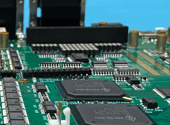
- Metal Shielding Cans: Metal cans can be placed over sensitive components or entire sections of the PCB to contain EMI. These cans are typically made of materials like aluminum or copper and are connected to the ground plane.
- Conductive Coatings: Conductive coatings, such as copper or silver, can be applied to the surface of the PCB to create a shield that blocks EMI.
- Shielded Enclosures: In some cases, the entire PCB may be placed inside a shielded enclosure to prevent EMI from escaping or entering.
2. Filtering
- Ferrite Beads: Ferrite beads can be placed on power lines or signal cables to filter out high-frequency noise.
- EMI Filters: EMI filters can be used to suppress conducted EMI on power lines or signal cables.
3. Grounding
- Star Grounding: In star grounding, all ground connections are routed to a single point, reducing ground loops and minimizing EMI.
- Ground Plane Segmentation: In some cases, segmenting the ground plane can help contain EMI within specific areas of the PCB.
Best Practices for PCB EMI Shielding
1. Early Consideration of EMI in Design
EMI considerations should be integrated into the PCB design process from the very beginning. This includes selecting components with low EMI characteristics, planning the layout to minimize EMI, and considering the use of shielding and filtering techniques.
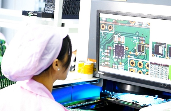
2. Simulation and Testing
- EMI Simulation: EMI simulation tools can be used to predict EMI issues before the PCB is manufactured. These tools can help identify potential problem areas and allow designers to make adjustments before the design is finalized.
- EMI Testing: EMI testing should be conducted on prototypes to verify that the design meets regulatory requirements and performs as expected. Testing should include both radiated and conducted EMI measurements.
3. Compliance with Standards
Designers should be familiar with the relevant EMI standards and regulations for their industry and region. Compliance with these standards is essential for ensuring that the final product can be legally sold and used.
4. Continuous Improvement
EMI shielding is an ongoing process. As new technologies and materials become available, designers should continuously evaluate and update their EMI shielding techniques to ensure the best possible performance.
Conclusion
EMI shielding is a critical aspect of PCB design that cannot be overlooked. By understanding the sources of EMI and implementing effective prevention and containment techniques, designers can ensure the reliable operation of their electronic devices. Early consideration of EMI, thorough simulation and testing, compliance with standards, and a commitment to continuous improvement are all essential components of a successful EMI shielding strategy. With the right approach, designers can minimize EMI and create high-performance, reliable PCBs that meet the demands of today’s complex electronic systems.