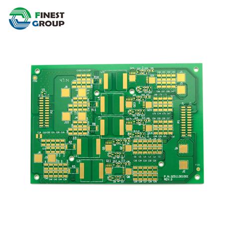
PCB EMI Simulation: A Comprehensive Guide to Reducing Electromagnetic Interference in Electronic Designs
Electromagnetic interference (EMI) is a critical concern in the design of modern electronic devices. As electronic systems become more complex and operate at higher frequencies, the risk of EMI increases, potentially leading to performance degradation, regulatory non-compliance, and even device failure. To address these challenges, engineers rely on PCB EMI simulation tools to predict, analyze, and mitigate EMI issues during the design phase. This article provides an in-depth exploration of PCB EMI simulation, its importance, methodologies, and best practices for ensuring EMI compliance and optimal performance.
What Is EMI and Why Is It Important?
Electromagnetic interference (EMI) refers to the disruption of electronic devices caused by electromagnetic radiation emitted from other devices or components. EMI can manifest as:
- Radiated EMI: Electromagnetic waves that propagate through the air and interfere with nearby devices.
- Conducted EMI: Noise that travels through conductive paths, such as power lines or signal traces.
EMI can lead to:
- Signal integrity issues, such as crosstalk and noise.
- Malfunction or failure of electronic systems.
- Non-compliance with regulatory standards (e.g., FCC, CISPR, IEC).
Given the increasing density and speed of modern PCBs, EMI has become a significant design challenge, making simulation an essential tool for identifying and addressing potential issues early in the design process.
The Role of PCB EMI Simulation
PCB EMI simulation is a computational process that predicts the electromagnetic behavior of a PCB design. By simulating the PCB’s electrical and magnetic fields, engineers can identify potential sources of EMI and evaluate the effectiveness of mitigation strategies. Key benefits of PCB EMI simulation include:
- Early Detection of EMI Issues:
- Simulation allows engineers to identify EMI problems during the design phase, reducing the need for costly redesigns and prototypes.
- Optimization of PCB Layout:
- By analyzing the impact of trace routing, component placement, and grounding strategies, engineers can optimize the PCB layout to minimize EMI.
- Compliance with Regulatory Standards:
- Simulation helps ensure that the PCB design meets EMI/EMC (electromagnetic compatibility) standards, reducing the risk of non-compliance.
- Improved Signal Integrity:
- EMI simulation helps identify and mitigate sources of noise and crosstalk, improving overall signal integrity.
- Cost and Time Savings:
- Addressing EMI issues early in the design process reduces the need for physical testing and redesigns, saving time and money.

Key Factors Influencing EMI in PCBs
To effectively simulate and mitigate EMI, engineers must understand the factors that contribute to EMI in PCB designs. These include:
- High-Speed Signals:
- High-frequency signals, such as those in clock circuits or data buses, are major sources of radiated EMI.
- Trace Routing:
- Poor routing practices, such as long parallel traces or sharp bends, can increase crosstalk and radiation.
- Component Placement:
- Improper placement of components, especially high-speed or high-power devices, can create EMI hotspots.
- Grounding and Shielding:
- Inadequate grounding or shielding can allow EMI to propagate through the PCB or escape into the environment.
- Power Distribution Network (PDN):
- Noise in the power supply can couple into signal traces, causing conducted EMI.
- Layer Stackup:
- The arrangement of signal, ground, and power layers in a multilayer PCB affects EMI performance.
- Edge Radiation:
- The edges of a PCB can act as antennas, radiating EMI into the surrounding environment.

Methodologies for PCB EMI Simulation
PCB EMI simulation involves several methodologies, each suited to different aspects of EMI analysis. The most common approaches include:
1. Time-Domain Simulation
- Time-domain simulation analyzes the behavior of signals over time, making it useful for identifying transient EMI issues, such as switching noise or signal reflections.
- Tools like SPICE (Simulation Program with Integrated Circuit Emphasis) are commonly used for time-domain analysis.
2. Frequency-Domain Simulation
- Frequency-domain simulation focuses on the frequency characteristics of signals, making it ideal for analyzing radiated EMI and resonance effects.
- Tools like ANSYS HFSS (High-Frequency Structure Simulator) and CST Studio Suite are widely used for frequency-domain analysis.
3. Electromagnetic Field Solvers
- Field solvers simulate the electromagnetic fields generated by the PCB, providing detailed insights into radiation patterns and coupling effects.
- These tools are essential for analyzing radiated EMI and optimizing shielding strategies.
4. Signal Integrity Analysis
- Signal integrity tools analyze the impact of EMI on signal quality, helping engineers identify and mitigate issues such as crosstalk and impedance mismatches.
- Popular tools include Cadence Sigrity and Mentor Graphics HyperLynx.
5. Power Integrity Analysis
- Power integrity tools simulate the behavior of the power distribution network, identifying sources of conducted EMI and optimizing decoupling capacitor placement.
- Tools like ANSYS SIwave and Keysight ADS are commonly used for power integrity analysis.
Best Practices for PCB EMI Simulation
To achieve accurate and effective EMI simulation results, engineers should follow these best practices:
1. Start Early in the Design Process
- Incorporate EMI simulation early in the design process to identify and address potential issues before they become costly problems.
2. Use Accurate Models
- Ensure that component models, including ICs, connectors, and passive components, accurately represent their electrical behavior.
3. Simulate Real-World Conditions
- Include realistic operating conditions, such as temperature, humidity, and power supply variations, in the simulation.
4. Optimize PCB Layout
- Use simulation results to guide PCB layout decisions, such as trace routing, component placement, and grounding strategies.
5. Analyze Multiple Scenarios
- Simulate different operating modes and configurations to identify worst-case EMI scenarios.
6. Validate with Physical Testing
- Use physical testing, such as near-field scanning or anechoic chamber measurements, to validate simulation results and ensure accuracy.
7. Iterate and Refine
- Continuously refine the design based on simulation feedback, iterating until EMI performance meets requirements.
Tools for PCB EMI Simulation
Several software tools are available for PCB EMI simulation, each offering unique features and capabilities. Some of the most popular tools include:
- ANSYS HFSS:
- A high-frequency electromagnetic field solver for analyzing radiated EMI and optimizing antenna designs.
- CST Studio Suite:
- A comprehensive electromagnetic simulation tool for analyzing EMI, signal integrity, and thermal effects.
- Cadence Sigrity:
- A signal and power integrity tool for analyzing EMI and optimizing PCB designs.
- Mentor Graphics HyperLynx:
- A suite of tools for signal integrity, power integrity, and EMI analysis.
- Keysight ADS (Advanced Design System):
- A versatile simulation platform for EMI, signal integrity, and RF/microwave design.
- Altium Designer:
- A PCB design tool with built-in signal integrity and EMI analysis capabilities.
Case Studies: PCB EMI Simulation in Action
1. High-Speed Digital Design:
- A company designing a high-speed digital PCB used EMI simulation to identify crosstalk between parallel traces. By rerouting the traces and adding ground planes, they reduced EMI and improved signal integrity.
2. RF Communication System:
- An RF communication system experienced radiated EMI due to improper grounding. Simulation revealed the issue, and the design was optimized with additional shielding and ground vias.
3. Automotive Electronics:
- An automotive electronics manufacturer used EMI simulation to ensure compliance with CISPR 25 standards. By optimizing the PCB layout and power distribution network, they achieved EMI compliance without costly redesigns.
Conclusion
PCB EMI simulation is an indispensable tool for modern electronics design, enabling engineers to predict, analyze, and mitigate EMI issues before they impact performance or compliance. By leveraging advanced simulation tools and following best practices, designers can create PCBs that meet the demands of high-speed, high-frequency applications while minimizing EMI risks.
As electronic systems continue to evolve, the importance of EMI simulation will only grow. By integrating simulation into the design process, engineers can ensure that their products deliver reliable performance, comply with regulatory standards, and stand out in a competitive market. Whether you’re designing consumer electronics, automotive systems, or aerospace technology, PCB EMI simulation is a critical step toward achieving success.